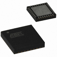
AT90PWM3-16MQ Atmel, AT90PWM3-16MQ Datasheet - Page 187
AT90PWM3-16MQ
Manufacturer Part Number
AT90PWM3-16MQ
Description
IC AVR MCU FLASH 8K 32QFN
Manufacturer
Atmel
Series
AVR® 90PWM Lightingr
Datasheet
1.AT90PWM3B-16SU.pdf
(361 pages)
Specifications of AT90PWM3-16MQ
Core Processor
AVR
Core Size
8-Bit
Speed
16MHz
Connectivity
SPI, UART/USART
Peripherals
Brown-out Detect/Reset, POR, PWM, WDT
Number Of I /o
27
Program Memory Size
8KB (8K x 8)
Program Memory Type
FLASH
Eeprom Size
512 x 8
Ram Size
512 x 8
Voltage - Supply (vcc/vdd)
2.7 V ~ 5.5 V
Data Converters
A/D 11x10b; D/A 1x10b
Oscillator Type
Internal
Operating Temperature
-40°C ~ 105°C
Package / Case
32-QFN
Processor Series
AT90PWMx
Core
AVR8
Data Bus Width
8 bit
Data Ram Size
512 B
Interface Type
SPI, USART
Maximum Clock Frequency
16 MHz
Number Of Programmable I/os
27
Number Of Timers
2
Operating Supply Voltage
2.7 V to 5.5 V
Maximum Operating Temperature
+ 105 C
Mounting Style
SMD/SMT
3rd Party Development Tools
EWAVR, EWAVR-BL
Development Tools By Supplier
ATAVRDRAGON, ATSTK500, ATSTK600, ATAVRISP2, ATAVRONEKIT, ATAVRFBKIT, ATAVRISP2
Minimum Operating Temperature
- 40 C
On-chip Adc
10 bit, 11 Channel
On-chip Dac
10 bit, 1 Channel
For Use With
ATSTK600-SOIC - STK600 SOCKET/ADAPTER FOR SOICATAVRMC200 - KIT EVAL FOR AT90PWM3 ASYNCATAVRFBKIT - KIT DEMO BALLAST FOR AT90PWM2ATAVRISP2 - PROGRAMMER AVR IN SYSTEMATSTK520 - ADAPTER KIT FOR 90PWM
Lead Free Status / RoHS Status
Lead free / RoHS Compliant
Available stocks
Company
Part Number
Manufacturer
Quantity
Price

Company:
Part Number:
AT90PWM3-16MQT
Manufacturer:
Atmel
Quantity:
1 325


18.3.4
18.4
18.4.1
4317J–AVR–08/10
Serial Frame
Synchronous Clock Operation
Frame Formats
Note that
to add some margin to avoid possible loss of data due to frequency variations.
When synchronous mode is used (UMSEL = 1), the XCK pin will be used as either clock input
(Slave) or clock output (Master). The dependency between the clock edges and data sampling
or data change is the same. The basic principle is that data input (on RxD) is sampled at the
opposite XCK clock edge of the edge the data output (TxDn) is changed.
Figure 18-3. Synchronous Mode XCK Timing.
The UCPOL bit UCRSnC selects which XCK clock edge is used for data sampling and which is
used for data change. As
rising XCK edge and sampled at falling XCK edge. If UCPOL is set, the data will be changed at
falling XCK edge and sampled at rising XCK edge.
A serial frame is defined to be one character of data bits with synchronization bits (start and stop
bits), and optionally a parity bit for error checking.
The USART accepts all 30 combinations of the following as valid frame formats:
•
•
•
•
A frame starts with the start bit followed by the least significant data bit. Then the next data bits,
up to a total of nine, are succeeding, ending with the most significant bit. If enabled, the parity bit
is inserted after the data bits, before the stop bits. When a complete frame is transmitted, it can
be directly followed by a new frame, or the communication line can be set to an idle (high) state.
Figure 18-4
optional.
1 start bit
5, 6, 7, 8, or 9 data bits
no, even or odd parity bit
1 or 2 stop bits
f
clk
UCPOLn = 1
UCPOLn = 0
illustrates the possible combinations of the frame formats. Bits inside brackets are
io
depends on the stability of the system clock source. It is therefore recommended
RxDn / TxDn
RxDn / TxDn
XCKn
XCKn
Figure 18-3
shows, when UCPOL is zero the data will be changed at
AT90PWM2/3/2B/3B
Sample
Sample
187
Related parts for AT90PWM3-16MQ
Image
Part Number
Description
Manufacturer
Datasheet
Request
R

Part Number:
Description:
IC AVR MCU FLASH 8K 32SOIC
Manufacturer:
Atmel
Datasheet:

Part Number:
Description:
MCU AVR 8K FLASH 16MHZ 32-QFN
Manufacturer:
Atmel
Datasheet:

Part Number:
Description:
DEV KIT FOR AVR/AVR32
Manufacturer:
Atmel
Datasheet:

Part Number:
Description:
INTERVAL AND WIPE/WASH WIPER CONTROL IC WITH DELAY
Manufacturer:
ATMEL Corporation
Datasheet:
Part Number:
Description:
Low-Voltage Voice-Switched IC for Hands-Free Operation
Manufacturer:
ATMEL Corporation
Datasheet:
Part Number:
Description:
MONOLITHIC INTEGRATED FEATUREPHONE CIRCUIT
Manufacturer:
ATMEL Corporation
Datasheet:
Part Number:
Description:
AM-FM Receiver IC U4255BM-M
Manufacturer:
ATMEL Corporation
Datasheet:
Part Number:
Description:
Monolithic Integrated Feature Phone Circuit
Manufacturer:
ATMEL Corporation
Datasheet:
Part Number:
Description:
Multistandard Video-IF and Quasi Parallel Sound Processing
Manufacturer:
ATMEL Corporation
Datasheet:
Part Number:
Description:
High-performance EE PLD
Manufacturer:
ATMEL Corporation
Datasheet:
Part Number:
Description:
8-bit Flash Microcontroller
Manufacturer:
ATMEL Corporation
Datasheet:
Part Number:
Description:
2-Wire Serial EEPROM
Manufacturer:
ATMEL Corporation
Datasheet: