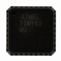
ATTINY88-MU Atmel, ATTINY88-MU Datasheet - Page 3

ATTINY88-MU
Manufacturer Part Number
ATTINY88-MU
Description
MCU AVR 8K ISP FLASH 1.8V 32-QFN
Manufacturer
Atmel
Series
AVR® ATtinyr
Specifications of ATTINY88-MU
Core Processor
AVR
Core Size
8-Bit
Speed
12MHz
Connectivity
I²C, SPI
Peripherals
Brown-out Detect/Reset, POR, WDT
Number Of I /o
28
Program Memory Size
8KB (4K x 16)
Program Memory Type
FLASH
Eeprom Size
64 x 8
Ram Size
512 x 8
Voltage - Supply (vcc/vdd)
1.8 V ~ 5.5 V
Data Converters
A/D 8x10b
Oscillator Type
Internal
Operating Temperature
-40°C ~ 85°C
Package / Case
32-VQFN Exposed Pad, 32-HVQFN, 32-SQFN, 32-DHVQFN
Processor Series
ATTINY8x
Core
AVR8
Data Bus Width
8 bit
Data Ram Size
512 B
Interface Type
2-Wire, I2S, SPI
Maximum Clock Frequency
12 MHz
Number Of Programmable I/os
28
Number Of Timers
2
Maximum Operating Temperature
+ 85 C
Mounting Style
SMD/SMT
3rd Party Development Tools
EWAVR, EWAVR-BL
Development Tools By Supplier
ATAVRDRAGON, ATSTK500, ATSTK600, ATAVRISP2, ATAVRONEKIT, ATQT600, ATAVRTS2080B
Minimum Operating Temperature
- 40 C
On-chip Adc
10 bit, 8 Channel
Package
32QFN EP
Device Core
AVR
Family Name
ATtiny
Maximum Speed
12 MHz
Operating Supply Voltage
2.5|3.3|5 V
Cpu Family
ATtiny
Device Core Size
8b
Frequency (max)
12MHz
Total Internal Ram Size
512Byte
# I/os (max)
28
Number Of Timers - General Purpose
2
Operating Supply Voltage (typ)
2.5/3.3/5V
Operating Supply Voltage (max)
5.5V
Operating Supply Voltage (min)
1.8V
Instruction Set Architecture
RISC
Operating Temp Range
-40C to 85C
Operating Temperature Classification
Industrial
Mounting
Surface Mount
Pin Count
32
Package Type
QFN EP
For Use With
ATSTK600-DIP40 - STK600 SOCKET/ADAPTER 40-PDIPATAVRDRAGON - KIT DRAGON 32KB FLASH MEM AVR
Lead Free Status / RoHS Status
Lead free / RoHS Compliant
Available stocks
Company
Part Number
Manufacturer
Quantity
Price
Company:
Part Number:
ATTINY88-MU
Manufacturer:
ATMEL
Quantity:
21 342
Part Number:
ATTINY88-MU
Manufacturer:
ATMEL/爱特梅尔
Quantity:
20 000
Part Number:
ATTINY88-MUR
Manufacturer:
AT
Quantity:
20 000
1.1
1.1.1
1.1.2
1.1.3
1.1.4
1.1.5
1.1.6
1.1.7
8008G–AVR–04/11
Pin Descriptions
VCC
AVCC
GND
Port A (PA3:0)
Port B (PB7:0)
Port C (PC7, PC5:0)
PC6/RESET
Digital supply voltage.
AV
be externally connected to V
mended this pin is connected to V
Canceling Techniques” on page
The following pins receive their supply voltage from AV
ages) PA[1:0]. All other I/O pins take their supply voltage from V
Ground.
Port A is a 4-bit bi-directional I/O port with internal pull-up resistors (selected for each bit). The
PA[3:0] output buffers have symmetrical drive characteristics with both sink and source capabil-
ity. As inputs, Port A pins that are externally pulled low will source current if the pull-up resistors
are activated. The Port A pins are tri-stated when a reset condition becomes active, even if the
clock is not running.
This port is available in 32-lead TQFP, 32-pad QFN and 32-ball UFBGA packages, only.
Port B is an 8-bit bi-directional I/O port with internal pull-up resistors (selected for each bit). The
Port B output buffers have symmetrical drive characteristics with both sink and source capability.
As inputs, Port B pins that are externally pulled low will source current if the pull-up resistors are
activated. The Port B pins are tri-stated when a reset condition becomes active, even if the clock
is not running.
Depending on the clock selection fuse settings, PB6 can be used as input to the internal clock
operating circuit.
The various special features of Port B are elaborated in
69.
Port C is a 8-bit bi-directional I/O port with internal pull-up resistors (selected for each bit). The
PC7 and PC[5:0] output buffers have symmetrical drive characteristics with both sink and source
capability. As inputs, Port C pins that are externally pulled low will source current if the pull-up
resistors are activated. The Port C pins are tri-stated when a reset condition becomes active,
even if the clock is not running.
If the RSTDISBL Fuse is programmed, PC6 is used as an I/O pin. Note that the electrical char-
acteristics of PC6 differ from those of the other pins of Port C.
If the RSTDISBL Fuse is unprogrammed, PC6 is used as a reset input. A low level on this pin for
longer than the minimum pulse width will generate a reset, even if the clock is not running. The
CC
is the supply voltage pin for the A/D converter and a selection of I/O pins. This pin should
CC
172.
even if the ADC is not used. If the ADC is used, it is recom-
CC
through a low-pass filter, as described in
CC
“Alternate Functions of Port B” on page
: PC7, PC[5:0] and (in 32-lead pack-
CC
.
ATtiny48/88
“Analog Noise
3


