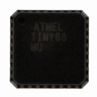
ATTINY88-MU Atmel, ATTINY88-MU Datasheet - Page 199

ATTINY88-MU
Manufacturer Part Number
ATTINY88-MU
Description
MCU AVR 8K ISP FLASH 1.8V 32-QFN
Manufacturer
Atmel
Series
AVR® ATtinyr
Specifications of ATTINY88-MU
Core Processor
AVR
Core Size
8-Bit
Speed
12MHz
Connectivity
I²C, SPI
Peripherals
Brown-out Detect/Reset, POR, WDT
Number Of I /o
28
Program Memory Size
8KB (4K x 16)
Program Memory Type
FLASH
Eeprom Size
64 x 8
Ram Size
512 x 8
Voltage - Supply (vcc/vdd)
1.8 V ~ 5.5 V
Data Converters
A/D 8x10b
Oscillator Type
Internal
Operating Temperature
-40°C ~ 85°C
Package / Case
32-VQFN Exposed Pad, 32-HVQFN, 32-SQFN, 32-DHVQFN
Processor Series
ATTINY8x
Core
AVR8
Data Bus Width
8 bit
Data Ram Size
512 B
Interface Type
2-Wire, I2S, SPI
Maximum Clock Frequency
12 MHz
Number Of Programmable I/os
28
Number Of Timers
2
Maximum Operating Temperature
+ 85 C
Mounting Style
SMD/SMT
3rd Party Development Tools
EWAVR, EWAVR-BL
Development Tools By Supplier
ATAVRDRAGON, ATSTK500, ATSTK600, ATAVRISP2, ATAVRONEKIT, ATQT600, ATAVRTS2080B
Minimum Operating Temperature
- 40 C
On-chip Adc
10 bit, 8 Channel
Package
32QFN EP
Device Core
AVR
Family Name
ATtiny
Maximum Speed
12 MHz
Operating Supply Voltage
2.5|3.3|5 V
Cpu Family
ATtiny
Device Core Size
8b
Frequency (max)
12MHz
Total Internal Ram Size
512Byte
# I/os (max)
28
Number Of Timers - General Purpose
2
Operating Supply Voltage (typ)
2.5/3.3/5V
Operating Supply Voltage (max)
5.5V
Operating Supply Voltage (min)
1.8V
Instruction Set Architecture
RISC
Operating Temp Range
-40C to 85C
Operating Temperature Classification
Industrial
Mounting
Surface Mount
Pin Count
32
Package Type
QFN EP
For Use With
ATSTK600-DIP40 - STK600 SOCKET/ADAPTER 40-PDIPATAVRDRAGON - KIT DRAGON 32KB FLASH MEM AVR
Lead Free Status / RoHS Status
Lead free / RoHS Compliant
Available stocks
Company
Part Number
Manufacturer
Quantity
Price
Company:
Part Number:
ATTINY88-MU
Manufacturer:
ATMEL
Quantity:
21 342
Part Number:
ATTINY88-MU
Manufacturer:
ATMEL/爱特梅尔
Quantity:
20 000
Part Number:
ATTINY88-MUR
Manufacturer:
AT
Quantity:
20 000
- Current page: 199 of 302
- Download datasheet (9Mb)
21.2.11
21.2.12
8008G–AVR–04/11
Programming the Lock Bits
Reading Fuse and Lock Bits
Figure 21-5. Programming the FUSES Waveforms
The algorithm for programming the lock bits is as follows (see
194
Lock bits can only be cleared by executing Chip Erase.
The algorithm for reading fuse and lock bits is as follows (see
194
Fuse and lock bit mapping is illustrated in
RESET +12V
• A: Load command “0010 0000”
• C: Load data low byte. Bit n = “0” programs the Lock bit. If LB1 and LB2 have been
• Give WR a negative pulse and wait for RDY/BSY to go high
• A: Load command “0000 0100”
• Set OE to “0”, BS2 to “0” and BS1 to “0”. Low fuse bits can now be read at DATA (“0” means
• Set OE to “0”, BS2 to “1” and BS1 to “1”. High fuse bits can now be read at DATA (“0” means
• Set OE to “0”, BS2 to “1”, and BS1 to “0”. Extended fuse bits can now be read at DATA (“0”
• Set OE to “0”, BS2 to “0” and BS1 to “1”. Lock bits can now be read at DATA (“0” means
• Set OE to “1”
RDY/BSY
programmed, it is not possible to program the Lock Bits by any External Programming mode
programmed)
programmed)
means programmed)
programmed)
PAGEL
for details on command and data loading):
for details on command loading):
CLKI
DATA
XA1
XA0
BS1
BS2
WR
OE
0x40
A
DATA
C
Write Fuse Low byte
XX
0x40
A
Figure
DATA
C
21-6, below.
Write Fuse high byte
XX
“Programming the Flash” on page
“Programming the Flash” on page
0x40
A
ATtiny48/88
DATA
C
Write Extended Fuse byte
XX
199
Related parts for ATTINY88-MU
Image
Part Number
Description
Manufacturer
Datasheet
Request
R

Part Number:
Description:
IC, MCU, 8BIT, 2K FLASH, 20SOIC
Manufacturer:
Atmel
Datasheet:

Part Number:
Description:
IC, MCU, 8BIT, 2K FLASH, 20PDIP
Manufacturer:
Atmel
Datasheet:

Part Number:
Description:
IC, MCU, 8BIT, 8K FLASH, 20PDIP
Manufacturer:
Atmel
Datasheet:

Part Number:
Description:
IC, MCU, 8BIT, 8K FLASH, 20SOIC
Manufacturer:
Atmel
Datasheet:

Part Number:
Description:
DEV KIT FOR AVR/AVR32
Manufacturer:
Atmel
Datasheet:

Part Number:
Description:
INTERVAL AND WIPE/WASH WIPER CONTROL IC WITH DELAY
Manufacturer:
ATMEL Corporation
Datasheet:

Part Number:
Description:
Low-Voltage Voice-Switched IC for Hands-Free Operation
Manufacturer:
ATMEL Corporation
Datasheet:

Part Number:
Description:
MONOLITHIC INTEGRATED FEATUREPHONE CIRCUIT
Manufacturer:
ATMEL Corporation
Datasheet:

Part Number:
Description:
AM-FM Receiver IC U4255BM-M
Manufacturer:
ATMEL Corporation
Datasheet:

Part Number:
Description:
Monolithic Integrated Feature Phone Circuit
Manufacturer:
ATMEL Corporation
Datasheet:

Part Number:
Description:
Multistandard Video-IF and Quasi Parallel Sound Processing
Manufacturer:
ATMEL Corporation
Datasheet:

Part Number:
Description:
High-performance EE PLD
Manufacturer:
ATMEL Corporation
Datasheet:


