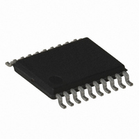
AT89LP4052-20XU Atmel, AT89LP4052-20XU Datasheet - Page 60

AT89LP4052-20XU
Manufacturer Part Number
AT89LP4052-20XU
Description
IC 8051 MCU FLASH 4K 20TSSOP
Manufacturer
Atmel
Series
89LPr
Datasheet
1.AT89LP2052-20PU.pdf
(94 pages)
Specifications of AT89LP4052-20XU
Core Processor
8051
Core Size
8-Bit
Speed
20MHz
Connectivity
SPI, UART/USART
Peripherals
Brown-out Detect/Reset, POR, PWM, WDT
Number Of I /o
15
Program Memory Size
4KB (4K x 8)
Program Memory Type
FLASH
Ram Size
256 x 8
Voltage - Supply (vcc/vdd)
2.4 V ~ 5.5 V
Oscillator Type
Internal
Operating Temperature
-40°C ~ 85°C
Package / Case
20-TSSOP
Processor Series
AT89x
Core
8051
Data Bus Width
8 bit
Data Ram Size
256 B
Interface Type
UART, SPI
Maximum Clock Frequency
20 MHz
Number Of Programmable I/os
15
Number Of Timers
2
Operating Supply Voltage
2.4 V to 5.5 V
Maximum Operating Temperature
+ 85 C
Mounting Style
SMD/SMT
3rd Party Development Tools
PK51, CA51, A51, ULINK2
Development Tools By Supplier
AT89ISP
Minimum Operating Temperature
- 40 C
Package
20TSSOP
Device Core
8051
Family Name
AT89
Maximum Speed
20 MHz
Lead Free Status / RoHS Status
Lead free / RoHS Compliant
Eeprom Size
-
Data Converters
-
Lead Free Status / Rohs Status
Details
Figure 23-3. Parallel Write Command Sequence
Figure 23-4. Parallel Read Command Sequence
60
AT89LP2052/LP4052
XTAL1
XTAL1
CS
CS
P1
P1
Figure 23-2. Flash Parallel Programming Device Connections
Note:
While CS is high, the interface is reset to its default state and P1 is tri-stated. CS should be
brought low before the first byte of a command is issued, and should return high only after the
last byte of the command has been strobed.
mand sequence. Command, address, and data bytes are sampled from P1 on the rising edge of
the XTAL1 pulse.
and address bytes are sampled from P1 on the rising edge of the XTAL1 pulse. At the falling
edge of the fourth XTAL1 pulse the device enables P1 to output data. The data remains on P1
until CS is brought high. During reads the parallel programmer should tri-state P1 before the
negative edge of the fourth XTAL1 pulse to avoid bus contention.
AAh
AAh
Sampling of pin P3.1 (RDY/BSY) is optional. During Parallel Programming, P3.1 will be pulled low
while the device is busy. Note that it does not require an external passive pull-up to V
R DY/BSY
Figure 23-4
OPCODE
OPCODE
CS
shows a generic parallel read command sequence. Command
ADDRH
ADDRH
AT89LP2052/LP4052
P3.1
P3.2
X TAL 1
GND
Figure 23-3
ADDRL
ADDRL
VCC
RST
P1
shows a generic parallel write com-
DATAIN
2.7 to 5.5V
DATAOUT
DATA
V PP
3547J–MICRO–10/09
CC
.


