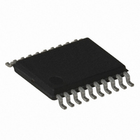
AT89LP4052-20XU Atmel, AT89LP4052-20XU Datasheet - Page 30

AT89LP4052-20XU
Manufacturer Part Number
AT89LP4052-20XU
Description
IC 8051 MCU FLASH 4K 20TSSOP
Manufacturer
Atmel
Series
89LPr
Datasheet
1.AT89LP2052-20PU.pdf
(94 pages)
Specifications of AT89LP4052-20XU
Core Processor
8051
Core Size
8-Bit
Speed
20MHz
Connectivity
SPI, UART/USART
Peripherals
Brown-out Detect/Reset, POR, PWM, WDT
Number Of I /o
15
Program Memory Size
4KB (4K x 8)
Program Memory Type
FLASH
Ram Size
256 x 8
Voltage - Supply (vcc/vdd)
2.4 V ~ 5.5 V
Oscillator Type
Internal
Operating Temperature
-40°C ~ 85°C
Package / Case
20-TSSOP
Processor Series
AT89x
Core
8051
Data Bus Width
8 bit
Data Ram Size
256 B
Interface Type
UART, SPI
Maximum Clock Frequency
20 MHz
Number Of Programmable I/os
15
Number Of Timers
2
Operating Supply Voltage
2.4 V to 5.5 V
Maximum Operating Temperature
+ 85 C
Mounting Style
SMD/SMT
3rd Party Development Tools
PK51, CA51, A51, ULINK2
Development Tools By Supplier
AT89ISP
Minimum Operating Temperature
- 40 C
Package
20TSSOP
Device Core
8051
Family Name
AT89
Maximum Speed
20 MHz
Lead Free Status / RoHS Status
Lead free / RoHS Compliant
Eeprom Size
-
Data Converters
-
Lead Free Status / Rohs Status
Details
16.6
17. External Interrupts
30
Timer/Counter Pin Configuration
AT89LP2052/LP4052
Figure 16-6. Timer/Counter 1 PWM Mode 0
Figure 16-7. Timer/Counter 1 PWM Mode 1
In order to use the counter input function or pulse width modulation output feature of Timer 0 or
Timer 1, the Timer pins T0 (P3.4) and T1 (P3.5) must be configured appropriately. See
15.7 “Port Alternate Functions” on page
should be configured as input-only, or as bidirectional with P3.4 or P3.5 set to “1”. The counter
function may also be triggered by an internal event if T0 or T1 is configured in a bidirectional or
output mode and the port bit is toggled accordingly. To enable a PWM output on T0 or T1, the
pin must be configured in a bidirectional or output mode with P3.4 or P3.5 set to “1”. Setting the
PWM0EN or PWM1En bits in TCONB will not automatically configure the pins as outputs. The
PWM outputs will use a full CMOS push-pull driver if they are in the quasi-bidirectional or output
configurations.
The INT0 and INT1 external interrupt sources can be programmed to be level-activated or tran-
sition-activated by setting or clearing bit IT1 or IT0 in Register TCON. If ITx = 0, external
interrupt x is triggered by a detected low at the INTx pin. If ITx = 1, external interrupt x is nega-
tive edge-triggered. In this mode if successive samples of the INTx pin show a high in one cycle
INT1 Pin
INT1 Pin
GATE
GATE
TR1
TR1
OSC
OSC
Control
Control
23. For the external counter input function, T0 or T1
PSC1
(8 Bits)
(8 Bits)
RL1
TL1
(8 Bits)
TL1
(8 Bits)
(8 Bits)
OCR1
(8 Bits)
(8 Bits)
OCR1
RH1
TH1
RH1
TH1
=
=
3547J–MICRO–10/09
T1
T1
Section


