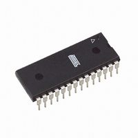
ATMEGA48A-PU Atmel, ATMEGA48A-PU Datasheet - Page 13

ATMEGA48A-PU
Manufacturer Part Number
ATMEGA48A-PU
Description
IC MCU AVR 4K FLASH 28PDIP
Manufacturer
Atmel
Series
AVR® ATmegar
Specifications of ATMEGA48A-PU
Core Processor
AVR
Core Size
8-Bit
Speed
20MHz
Connectivity
I²C, SPI, UART/USART
Peripherals
Brown-out Detect/Reset, POR, PWM, WDT
Number Of I /o
23
Program Memory Size
4KB (2K x 16)
Program Memory Type
FLASH
Eeprom Size
256 x 8
Ram Size
512 x 8
Voltage - Supply (vcc/vdd)
1.8 V ~ 5.5 V
Data Converters
A/D 6x10b
Oscillator Type
Internal
Operating Temperature
-40°C ~ 85°C
Package / Case
28-DIP (0.300", 7.62mm)
Controller Family/series
Atmega
No. Of I/o's
23
Eeprom Memory Size
256Byte
Ram Memory Size
512Byte
Cpu Speed
20MHz
Rohs Compliant
Yes
Lead Free Status / RoHS Status
Lead free / RoHS Compliant
- Current page: 13 of 566
- Download datasheet (23Mb)
6.5.1
6.6
8271C–AVR–08/10
Instruction Execution Timing
SPH and SPL – Stack Pointer High and Stack Pointer Low Register
This section describes the general access timing concepts for instruction execution. The AVR
CPU is driven by the CPU clock clk
chip. No internal clock division is used.
Figure 6-4
vard architecture and the fast-access Register File concept. This is the basic pipelining concept
to obtain up to 1 MIPS per MHz with the corresponding unique results for functions per cost,
functions per clocks, and functions per power-unit.
Figure 6-4.
Figure 6-5
operation using two register operands is executed, and the result is stored back to the destina-
tion register.
Figure 6-5.
ATmega48A/48PA/88A/88PA/168A/168PA/328/328
Bit
0x3E (0x5E)
0x3D (0x5D)
Read/Write
Initial Value
Register Operands Fetch
2nd Instruction Execute
3rd Instruction Execute
1st Instruction Execute
ALU Operation Execute
2nd Instruction Fetch
3rd Instruction Fetch
4th Instruction Fetch
1st Instruction Fetch
Total Execution Time
shows the internal timing concept for the Register File. In a single clock cycle an ALU
shows the parallel instruction fetches and instruction executions enabled by the Har-
Result Write Back
RAMEND
RAMEND
SP15
The Parallel Instruction Fetches and Instruction Executions
Single Cycle ALU Operation
SP7
R/W
R/W
15
7
clk
clk
CPU
RAMEND
RAMEND
CPU
SP14
SP6
R/W
R/W
14
6
RAMEND
RAMEND
SP13
R/W
R/W
SP5
13
5
CPU
T1
T1
, directly generated from the selected clock source for the
RAMEND
RAMEND
SP12
R/W
R/W
SP4
12
4
RAMEND
RAMEND
SP11
R/W
R/W
SP3
T2
11
T2
3
RAMEND
RAMEND
SP10
SP2
R/W
R/W
10
2
T3
T3
RAMEND
RAMEND
SP9
SP1
R/W
R/W
9
1
RAMEND
RAMEND
SP8
SP0
R/W
R/W
8
0
T4
T4
SPH
SPL
13
Related parts for ATMEGA48A-PU
Image
Part Number
Description
Manufacturer
Datasheet
Request
R

Part Number:
Description:
IC AVR MCU 4K 5V 20MHZ 32-TQFP
Manufacturer:
Atmel
Datasheet:

Part Number:
Description:
Manufacturer:
Atmel Corporation
Datasheet:

Part Number:
Description:
Manufacturer:
Atmel Corporation
Datasheet:

Part Number:
Description:
IC AVR MCU 4K 20MHZ 5V 32TQFP
Manufacturer:
Atmel
Datasheet:

Part Number:
Description:
IC AVR MCU 4K 20MHZ 5V 28DIP
Manufacturer:
Atmel
Datasheet:

Part Number:
Description:
IC AVR MCU 4K 20MHZ 5V 32-QFN
Manufacturer:
Atmel
Datasheet:

Part Number:
Description:
IC AVR MCU 4K 5V 20MHZ 32-TQFP
Manufacturer:
Atmel
Datasheet:

Part Number:
Description:
IC AVR MCU 4K 5V 20MHZ 32-QFN
Manufacturer:
Atmel
Datasheet:

Part Number:
Description:
IC AVR MCU 4K 5V 20MHZ 32-QFN
Manufacturer:
Atmel
Datasheet:

Part Number:
Description:
IC AVR MCU 4K 5V 20MHZ 28-DIP
Manufacturer:
Atmel
Datasheet:

Part Number:
Description:
IC AVR MCU 4K 5V 20MHZ 28-DIP
Manufacturer:
Atmel
Datasheet:

Part Number:
Description:
IC AVR MCU 4K FLASH 20MHZ 28QFN
Manufacturer:
Atmel
Datasheet:


