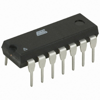
ATTINY24-20PU Atmel, ATTINY24-20PU Datasheet - Page 139

ATTINY24-20PU
Manufacturer Part Number
ATTINY24-20PU
Description
IC MCU AVR 2K FLASH 20MHZ 14-DIP
Manufacturer
Atmel
Series
AVR® ATtinyr
Specifications of ATTINY24-20PU
Core Processor
AVR
Core Size
8-Bit
Speed
20MHz
Connectivity
USI
Peripherals
Brown-out Detect/Reset, POR, PWM, Temp Sensor, WDT
Number Of I /o
12
Program Memory Size
2KB (1K x 16)
Program Memory Type
FLASH
Eeprom Size
128 x 8
Ram Size
128 x 8
Voltage - Supply (vcc/vdd)
2.7 V ~ 5.5 V
Data Converters
A/D 8x10b
Oscillator Type
Internal
Operating Temperature
-40°C ~ 85°C
Package / Case
14-DIP (0.300", 7.62mm)
Processor Series
ATTINY2x
Core
AVR8
Data Bus Width
8 bit
Data Ram Size
128 B
Interface Type
SPI
Maximum Clock Frequency
20 MHz
Number Of Programmable I/os
12
Number Of Timers
2
Operating Supply Voltage
2.7 V to 5.5 V
Maximum Operating Temperature
+ 85 C
Mounting Style
Through Hole
3rd Party Development Tools
EWAVR, EWAVR-BL
Development Tools By Supplier
ATAVRDRAGON, ATSTK500, ATSTK600, ATAVRISP2, ATAVRONEKIT
Minimum Operating Temperature
- 40 C
On-chip Adc
8-ch x 10-bit
For Use With
ATSTK600-DIP40 - STK600 SOCKET/ADAPTER 40-PDIP770-1007 - ISP 4PORT ATMEL AVR MCU SPI/JTAGATAVRISP2 - PROGRAMMER AVR IN SYSTEMATSTK505 - ADAPTER KIT FOR 14PIN AVR MCU
Lead Free Status / RoHS Status
Lead free / RoHS Compliant
- Current page: 139 of 238
- Download datasheet (5Mb)
16.6.2
16.7
16.8
8006K–AVR–10/10
ADC Noise Canceler
Analog Input Circuitry
ADC Voltage Reference
selection. Since the next conversion has already started automatically, the next result will reflect
the previous channel selection. Subsequent conversions will reflect the new channel selection.
The reference voltage for the ADC (V
ended channels that exceed V
either V
after switching reference voltage source may be inaccurate, and the user is advised to discard
this result.
The ADC features a noise canceler that enables conversion during sleep mode. This reduces
noise induced from the CPU core and other I/O peripherals. The noise canceler can be used
with ADC Noise Reduction and Idle mode. To make use of this feature, the following procedure
should be used:
Note that the ADC will not automatically be turned off when entering other sleep modes than Idle
mode and ADC Noise Reduction mode. The user is advised to write zero to ADEN before enter-
ing such sleep modes to avoid excessive power consumption.
The analog input circuitry for single ended channels is illustrated in
analog source applied to ADCn is subjected to the pin capacitance and input leakage of that pin,
regardless of whether that channel is selected as input for the ADC. When the channel is
selected, the source must drive the S/H capacitor through the series resistance (combined resis-
tance in the input path).
The ADC is optimized for analog signals with an output impedance of approximately 10kΩ or
less. If such a source is used, the sampling time will be negligible. If a source with higher imped-
ance is used, the sampling time will depend on how long time the source needs to charge the
S/H capacitor, which can vary widely. With slowly varying signals the user is recommended to
use sources with low impedance, only, since this minimizes the required charge transfer to the
S/H capacitor.
Signal components higher than the Nyquist frequency (f
distortion from unpredictable signal convolution. The user is advised to remove high frequency
components with a low-pass filter before applying the signals as inputs to the ADC.
• Make sure that the ADC is enabled and is not busy converting. Single Conversion mode must
• Enter ADC Noise Reduction mode (or Idle mode). The ADC will start a conversion once the
• If no other interrupts occur before the ADC conversion completes, the ADC interrupt will wake
be selected and the ADC conversion complete interrupt must be enabled.
CPU has been halted.
up the CPU and execute the ADC Conversion Complete interrupt routine. If another interrupt
wakes up the CPU before the ADC conversion is complete, that interrupt will be executed,
and an ADC Conversion Complete interrupt request will be generated when the ADC
conversion completes. The CPU will remain in active mode until a new sleep command is
executed.
CC
, or internal 1.1V reference, or external AREF pin. The first ADC conversion result
REF
will result in codes close to 0x3FF. V
REF
) indicates the conversion range for the ADC. Single
ADC
/2) should not be present to avoid
Figure 16-8 on page
ATtiny24/44/84
REF
can be selected as
140. An
139
Related parts for ATTINY24-20PU
Image
Part Number
Description
Manufacturer
Datasheet
Request
R

Part Number:
Description:
Manufacturer:
Atmel Corporation
Datasheet:

Part Number:
Description:
Manufacturer:
Atmel Corporation
Datasheet:

Part Number:
Description:
IC MCU AVR 2K FLASH 20MHZ 20-QFN
Manufacturer:
Atmel
Datasheet:

Part Number:
Description:
IC MCU AVR 2K FLASH 20MHZ 14SOIC
Manufacturer:
Atmel
Datasheet:

Part Number:
Description:
MCU AVR 2K FLASH 15MHZ 20-QFN
Manufacturer:
Atmel
Datasheet:

Part Number:
Description:
MCU AVR 2KB FLASH 20MHZ 14SOIC
Manufacturer:
Atmel
Datasheet:

Part Number:
Description:
MCU AVR 2KB FLASH 20MHZ 20QFN
Manufacturer:
Atmel
Datasheet:

Part Number:
Description:
MCU AVR 2K FLASH 15MHZ 14-SOIC
Manufacturer:
Atmel
Datasheet:

Part Number:
Description:
DEV KIT FOR AVR/AVR32
Manufacturer:
Atmel
Datasheet:

Part Number:
Description:
INTERVAL AND WIPE/WASH WIPER CONTROL IC WITH DELAY
Manufacturer:
ATMEL Corporation
Datasheet:

Part Number:
Description:
Low-Voltage Voice-Switched IC for Hands-Free Operation
Manufacturer:
ATMEL Corporation
Datasheet:

Part Number:
Description:
MONOLITHIC INTEGRATED FEATUREPHONE CIRCUIT
Manufacturer:
ATMEL Corporation
Datasheet:


