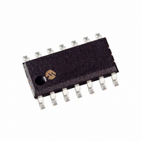
PIC16F616-I/SL Microchip Technology, PIC16F616-I/SL Datasheet - Page 6

PIC16F616-I/SL
Manufacturer Part Number
PIC16F616-I/SL
Description
IC PIC MCU FLASH 2KX14 14SOIC
Manufacturer
Microchip Technology
Series
PIC® 16Fr
Datasheets
1.PIC12F609T-ISN.pdf
(26 pages)
2.PIC16F616T-ISL.pdf
(4 pages)
3.PIC16F616T-ISL.pdf
(214 pages)
4.PIC16F616T-ISL.pdf
(8 pages)
5.PIC16F616-ESL.pdf
(180 pages)
Specifications of PIC16F616-I/SL
Program Memory Type
FLASH
Program Memory Size
3.5KB (2K x 14)
Package / Case
14-SOIC (3.9mm Width), 14-SOL
Core Processor
PIC
Core Size
8-Bit
Speed
20MHz
Peripherals
Brown-out Detect/Reset, POR, PWM, WDT
Number Of I /o
11
Ram Size
128 x 8
Voltage - Supply (vcc/vdd)
2 V ~ 5.5 V
Data Converters
A/D 8x10b
Oscillator Type
Internal
Operating Temperature
-40°C ~ 85°C
Processor Series
PIC16F
Core
PIC
Data Bus Width
8 bit
Data Ram Size
128 B
Maximum Clock Frequency
20 MHz
Number Of Programmable I/os
11
Number Of Timers
3
Maximum Operating Temperature
+ 85 C
Mounting Style
SMD/SMT
3rd Party Development Tools
52715-96, 52716-328, 52717-734
Development Tools By Supplier
PG164130, DV164035, DV244005, DV164005, PG164120, ICE2000
Minimum Operating Temperature
- 40 C
On-chip Adc
10 bit, 8 Channel
Lead Free Status / RoHS Status
Lead free / RoHS Compliant
For Use With
MCP1631RD-DCPC1 - REF DES BATT CHARG OR LED DRIVERAC162083 - HEADER MPLAB ICD2 PIC16F616 8/14
Eeprom Size
-
Connectivity
-
Lead Free Status / Rohs Status
Lead free / RoHS Compliant
Available stocks
Company
Part Number
Manufacturer
Quantity
Price
Company:
Part Number:
PIC16F616-I/SL
Manufacturer:
MICROCHIP
Quantity:
400
Company:
Part Number:
PIC16F616-I/SL
Manufacturer:
Microchip Technology
Quantity:
45 197
Part Number:
PIC16F616-I/SL
Manufacturer:
MICROCHIP
Quantity:
20 000
PIC12F609/12F615/12F617/16F610/16F616 AND PIC12HV609/12HV615/16HV610/16HV616
4.0
Two methods are available to enter Program/Verify
mode. “V
ICSPCLK low while raising the MCLR pin from V
V
method can be used for any Configuration Word selec-
tion and must be used if the INTOSC and internal
MCLR options are selected (FOSC<2:0> = 100 or 101
and MCLRE = 0). The V
device from executing code prior to entering Program/
Verify mode. See the timing diagram in Figure 4-1.
The second entry method, “V
applying V
then raising MCLR pin from V
followed by data. This method can be used for any
Configuration Word selection except when INTOSC
and internal MCLR options are selected (FOSC<2:0> =
100 or 101 and MCLRE = 0). This technique is useful
when programming the device when V
applied, for it is not necessary to disconnect V
enter Program/Verify mode. See the timing diagram in
Figure 4-2.
Once in Program/Verify mode, the program memory
and configuration memory can be accessed and
programmed in serial fashion. ICSPDAT and ICSPCLK
are Schmitt Trigger inputs in this mode. RA4 is tri-state
regardless of fuse setting.
The sequence that enters the device into the Program/
Verify mode places all other logic into the Reset state
(the MCLR pin was initially at V
are in the Reset state (high-impedance inputs) and the
PC is cleared.
To prevent a device configured with INTOSC and
internal MCLR from executing after exiting Program/
Verify mode, V
See Figure 4-3 for the timing.
FIGURE 4-1:
DS41396A-page 6
IHH
ICSPCLK
ICSPDAT
(high voltage), then applying V
Note:
V
V
DD
PP
PROGRAM/VERIFY MODE
PP
DD
-first” is entered by holding ICSPDAT and
, holding ICSPDAT and ICSPCLK low,
DD
This method of entry is valid, regardless
of Configuration Word selected.
needs to power down before V
T
PPDP
V
VERIFY MODE ENTRY
PP
-FIRST PROGRAM/
PP
T
-first entry prevents the
IL
HLD
DD
to V
IL
-first”, is entered by
0
). Therefore, all I/Os
IHH
DD
and data. This
(high voltage),
DD
is already
DD
IL
PP
to
to
.
FIGURE 4-2:
FIGURE 4-3:
4.1
The PIC16F616/PIC12F617 program memory may be
written in two ways. The fastest method writes four
words at a time. However, one-word writes are also
supported for backward compatibility with previous 8-
pin and 14-pin Flash devices. The four-word algorithm
is used to program the program memory only. The one-
word algorithm can write any available memory
location (i.e., program memory, configuration memory
and calibration memory).
After writing the array, the PC may be reset and read
back to verify the write. It is not possible to verify
immediately following the write because the PC can
only increment, not decrement.
A device Reset will clear the PC and set the address to
‘0’. The Increment Address command will increment
the PC. The Load Configuration command will set the
PC to 0x2000. The available commands are shown in
Table 4-1.
ICSPCLK
ICSPCLK
ICSPDAT
ICSPDAT
Note:
Note:
V
V
V
V
DD
DD
PP
PP
Program/Erase Algorithms
The PIC12F615, PIC12F609, PIC16F610
program memories must be written in
one-word writes only.
This method of entry is valid if INTOSC
and internal MCLR are not selected.
T
HLD
V
VERIFY MODE ENTRY
PROGRAM/VERIFY MODE
EXIT
T
2009 Microchip Technology Inc.
DD
0
HLD
-FIRST PROGRAM/
0
T
PPDP


