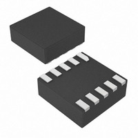
MAX13208EALB+T Maxim Integrated Products, MAX13208EALB+T Datasheet - Page 6

MAX13208EALB+T
Manufacturer Part Number
MAX13208EALB+T
Description
IC ESD PROTECTOR 8I/O 10UDFN
Manufacturer
Maxim Integrated Products
Datasheet
1.MAX13208EALBT.pdf
(9 pages)
Specifications of MAX13208EALB+T
Power (watts)
403mW
Polarization
8 Channel Array - Unidirectional
Mounting Type
Surface Mount
Package / Case
10-µDFN
Lead Free Status / RoHS Status
Lead free / RoHS Compliant
Voltage - Breakdown
-
Voltage - Reverse Standoff (typ)
-
Other names
MAX13208EALB+T
MAX13208EALB+TTR
MAX13208EALB+TTR
Figure 6. IEC 61000-4-2 ESD Test Model
Figure 4 shows the Human Body Model, and Figure 5
shows the current waveform it generates when dis-
charged into a low impedance. This model consists of
a 100pF capacitor charged to the ESD voltage of inter-
est, which is then discharged into the device through a
1.5kΩ resistor.
The IEC 61000-4-2 standard covers ESD testing and
performance of finished equipment. The MAX13202E/
MAX13204E/MAX13206E/MAX13208E help users
design equipment that meets Level 4 of IEC 61000-4-2.
The main difference between tests done using the
Human Body Model and IEC 61000-4-2 is higher peak
current in IEC 61000-4-2. Because series resistance is
lower in the IEC 61000-4-2 ESD test model (Figure 6),
the ESD-withstand voltage measured to this standard is
generally lower than that measured using the Human
Body Model. Figure 3 shows the current waveform for
the ±8kV IEC 61000-4-2 Level 4 ESD Contact
Discharge test.
The Air-Gap Discharge test involves approaching the
device with a charged probe. The Contact Discharge
method connects the probe to the device before the
probe is energized.
2-/4-/6-/8-Channel, ±30kV ESD Protectors in µDFN
6
VOLTAGE
SOURCE
_______________________________________________________________________________________
HIGH-
DC
CHARGE-CURRENT-
LIMIT RESISTOR
50Ω to 100Ω
R
C
150pF
C s
STORAGE
CAPACITOR
RESISTANCE
DISCHARGE
330Ω
R
D
Human Body Model
IEC 61000-4-2
DEVICE
UNDER
TEST
Proper circuit-board layout is critical to suppress ESD-
induced line transients. The MAX13202E/MAX13204E/
MAX13206E/MAX13208E clamp to ±120V; however, with
improper layout, the voltage spike at the device is much
higher. A lead inductance of 10nH with a 45A current
spike at a dv/dt of 1ns results in an ADDITIONAL 450V
spike on the protected line. It is essential that the layout
of the PC board follows these guidelines:
1) Minimize trace length between the connector or
2) Use separate planes for power and ground to reduce
3) Ensure short ESD transient return paths to GND
4) Minimize conductive power and ground loops.
5) Do not place critical signals near the edge of the
6) Bypass V
7) Bypass the supply of the protected device to GND
PROCESS: BiCMOS
input terminal, I/O_, and the protected signal line.
parasitic inductance and to reduce the impedance to
the power rails for shunted ESD current.
and V
PC board.
tor as close to V
with a low-ESR ceramic capacitor as close to the
supply pin as possible.
CC
.
CC
to GND with a low-ESR ceramic capaci-
CC
Layout Recommendations
and ground terminals as possible.
Chip Information


