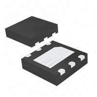
MAX3204EETT+T Maxim Integrated Products, MAX3204EETT+T Datasheet - Page 6

MAX3204EETT+T
Manufacturer Part Number
MAX3204EETT+T
Description
IC ESD PROT ARRAY 6-TDFN
Manufacturer
Maxim Integrated Products
Datasheet
1.MAX3202EETTT.pdf
(9 pages)
Specifications of MAX3204EETT+T
Power (watts)
1.95W
Polarization
4 Channel Array - Unidirectional
Mounting Type
Surface Mount
Package / Case
6-TDFN Exposed Pad
Lead Free Status / RoHS Status
Lead free / RoHS Compliant
Voltage - Breakdown
-
Voltage - Reverse Standoff (typ)
-
Lead Free Status / Rohs Status
Details
Other names
MAX3204EETT+T
MAX3204EETT+TTR
MAX3204EETT+TTR
Figure 6. IEC 61000-4-2 ESD Test Model
The IEC 61000-4-2 standard covers ESD testing and
performance of finished equipment. The MAX3202E/
MAX3203E/MAX3204E/MAX3206E help users design
equipment that meets Level 4 of IEC 61000-4-2.
The main difference between tests done using the
Human Body Model and IEC 61000-4-2 is higher peak
current in IEC 61000-4-2. Because series resistance is
lower in the IEC 61000-4-2 ESD test model (Figure 6)
the ESD-withstand voltage measured to this standard is
generally lower than that measured using the Human
Body Model. Figure 3 shows the current waveform for
the ±8kV IEC 61000-4-2 Level 4 ESD Contact
Discharge test.
The Air-Gap Discharge test involves approaching the
device with a charged probe. The Contact Discharge
method connects the probe to the device before the
probe is energized.
Proper circuit-board layout is critical to suppress ESD-
induced line transients. The MAX3202E/MAX3203E/
MAX3204E/MAX3206E clamp to 100V; however, with
improper layout, the voltage spike at the device is
much higher. A lead inductance of 10nH with a 45A
current spike at a dv/dt of 1ns results in an ADDITION-
AL 450V spike on the protected line. It is essential that
the layout of the PC board follows these guidelines:
1) Minimize trace length between the connector or
2) Use separate planes for power and ground to reduce
Low-Capacitance, 2/3/4/6-Channel, ±15kV ESD
Protection Arrays for High-Speed Data Interfaces
6
input terminal, I/O_, and the protected signal line.
parasitic inductance and to reduce the impedance to
the power rails for shunted ESD current.
VOLTAGE
SOURCE
_______________________________________________________________________________________
HIGH-
DC
CHARGE-CURRENT-
LIMIT RESISTOR
50Ω to 100Ω
R
C
150pF
C s
Layout Recommendations
STORAGE
CAPACITOR
RESISTANCE
DISCHARGE
330Ω
R
D
IEC 61000-4-2
DEVICE
UNDER
TEST
3) Ensure short ESD transient return paths to GND
4) Minimize conductive power and ground loops.
5) Do not place critical signals near the edge of the
6) Bypass V
7) Bypass the supply of the protected device to GND
For general UCSP package information and PC layout
considerations, refer to Maxim Application Note 263,
Wafer-Level Chip-Scale Package .
The UCSP represents a unique packaging form factor
that may not perform equally to a packaged product
through traditional mechanical reliability tests. UCSP
reliability is integrally linked to the user’s assembly meth-
ods, circuit-board material, and usage environment.
The user should closely review these areas when con-
sidering use of a UCSP. Performance through operat-
ing life test and moisture resistance remains
uncompromised as it is primarily determined by the
wafer-fabrication process. Mechanical stress perfor-
mance is a greater consideration for a UCSP. UCSPs
are attached through direct solder contact to the user’s
PC board, foregoing the inherent stress relief of a pack-
aged product lead frame. Solder-joint contact integrity
must be considered. Table 1 shows the testing done to
characterize the UCSP reliability performance. In con-
clusion, the UCSP is capable of performing reliably
through environmental stresses as indicated by the
results in the table. Additional usage data and recom-
mendations are detailed in the UCSP application note,
which can be found on Maxim’s website at
www.maxim-ic.com.
PROCESS: BiCMOS
___________________UCSP Reliability
and V
PC board.
itor as close to V
with a low-ESR ceramic capacitor as close to the
supply pin as possible.
CC
.
CC
to GND with a low-ESR ceramic capac-
CC
as possible.
UCSP Considerations
Chip Information


