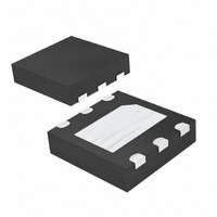
MAX3204EETT+T Maxim Integrated Products, MAX3204EETT+T Datasheet - Page 2

MAX3204EETT+T
Manufacturer Part Number
MAX3204EETT+T
Description
IC ESD PROT ARRAY 6-TDFN
Manufacturer
Maxim Integrated Products
Datasheet
1.MAX3202EETTT.pdf
(9 pages)
Specifications of MAX3204EETT+T
Power (watts)
1.95W
Polarization
4 Channel Array - Unidirectional
Mounting Type
Surface Mount
Package / Case
6-TDFN Exposed Pad
Lead Free Status / RoHS Status
Lead free / RoHS Compliant
Voltage - Breakdown
-
Voltage - Reverse Standoff (typ)
-
Lead Free Status / Rohs Status
Details
Other names
MAX3204EETT+T
MAX3204EETT+TTR
MAX3204EETT+TTR
ABSOLUTE MAXIMUM RATINGS
V
I/O_ to GND ................................................-0.3V to (V
Continuous Power Dissipation (T
Low-Capacitance, 2/3/4/6-Channel, ±15kV ESD
Protection Arrays for High-Speed Data Interfaces
Note 1: The UCSP devices are constructed using a unique set of packaging techniques that impose a limit on the thermal profile the
Stresses beyond those listed under “Absolute Maximum Ratings” may cause permanent damage to the device. These are stress ratings only, and functional
operation of the device at these or any other conditions beyond those indicated in the operational sections of the specifications is not implied. Exposure to
absolute maximum rating conditions for extended periods may affect device reliability.
ELECTRICAL CHARACTERISTICS
(V
Note 2: Limits over temperature are guaranteed by design, not production tested.
Note 3: Idealized clamp voltages (L1 = L2 = L3 = 0) (Figure 1 ); see the Applications Information section for more information.
Note 4: Guaranteed by design. Not production tested.
2
Supply Voltage
Supply Current
Diode Forward Voltage
Channel Clamp Voltage
(Note 3)
Channel Leakage Current
Channel Input Capacitance
ESD PROTECTION
Human Body Model
IEC 61000-4-2
Contact Discharge
IEC 61000-4-2
Air-Gap Discharge
CC
2 × 2 WLP (derate 11.5mW/°C above +70°C)...............920mW
3 × 2 UCSP (derate 3.4mW/°C above +70°C) ..............273mW
3 × 2 WLP (derate 12.3mW/°C above +70°C)...............984mW
3 × 3 WLP (derate 14.1mW/°C above +70°C).............1128mW
6-Pin TDFN (derate 24.4mW/°C above +70°C) ..........1951mW
12-Pin TQFN (derate 16.9mW/°C above +70°C) ........1349mW
CC
_______________________________________________________________________________________
to GND ...........................................................-0.3V to +7.0V
= +5V ±5%, T
PARAMETER
device can be exposed to during board-level solder attach and rework. This limit permits the use of only the solder profiles
recommended in the industry-standard specification, JEDEC 020A, paragraph 7.6, Table 3 for IR/VPR and Convection
Reflow. Preheating is required. Hand or wave soldering is not allowed.
A
= T
MIN
to T
SYMBOL
A
MAX
= +70°C)
V
I
V
V
CC
CC
C
, unless otherwise noted. Typical values are at V
F
I
T
Human Body Model,
I
T
Contact Discharge
(IEC 61000-4-2), I
T
Air-Gap Discharge
(IEC 61000-4-2), I
T
V
F
F
A
A
A
A
CC
= 10mA
= 10A
= +25°C, ±15kV
= +25°C, ±8kV
= +25°C, ±15kV
= 0°C to +50°C (Note 4)
= 5V, bias of V
CC
+ 0.3V)
F
F
CONDITIONS
= 24A
= 45A
CC
/2
Operating Temperature Range ...........................-40°C to +85°C
Storage Temperature Range .............................-65°C to +150°C
Junction Temperature .....................................................+150°C
Bump Temperature (soldering) (Note 1)
Lead Temperature (soldering, 10s) .................................+300°C
Infrared (15s) ................................................................+220°C
Vapor Phase (60s) ........................................................+215°C
Positive transients
Negative transients
Positive transients
Negative transients
Positive transients
Negative transients
CC
= +5V and T
0.65
MIN
0.9
-1
A
= +25°C.) (Note 2)
TYP
±15
±15
1
5
±8
V
V
V
CC
CC
CC
MAX
0.95
-100
100
5.5
-25
-60
+1
+ 100
7
+ 25
+ 60
UNITS
nA
nA
pF
kV
kV
kV
V
V
V


