SD12T1G ON Semiconductor, SD12T1G Datasheet - Page 2
SD12T1G
Manufacturer Part Number
SD12T1G
Description
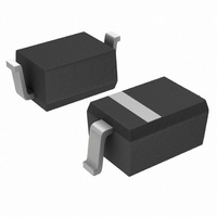
TVS ZENER 350W 12V ESD SOD323
Manufacturer
ON Semiconductor
Datasheet
1.SD05T1G.pdf
(4 pages)
Specifications of SD12T1G
Voltage - Reverse Standoff (typ)
12V
Voltage - Breakdown
13.3V
Power (watts)
350W
Polarization
Unidirectional
Mounting Type
Surface Mount
Package / Case
SC-76, SOD-323, UMD2
Polarity
Unidirectional
Channels
1 Channel
Clamping Voltage
25 V
Operating Voltage
12 V
Breakdown Voltage
13.3 V
Termination Style
SMD/SMT
Peak Surge Current
15 A
Peak Pulse Power Dissipation
350 W
Capacitance
150 pF
Maximum Operating Temperature
+ 150 C
Minimum Operating Temperature
- 55 C
Dimensions
1.25 mm W x 1.7 mm L
Dc
07+
Lead Free Status / RoHS Status
Lead free / RoHS Compliant
Other names
SD12T1GOS
SD12T1GOS
SD12T1GOSTR
SD12T1GOS
SD12T1GOSTR
Available stocks
Company
Part Number
Manufacturer
Quantity
Price
Company:

Part Number:
SD12T1G
Manufacturer:
ON Semiconductor
Quantity:
43 864
Company:
Part Number:
SD12T1G
Manufacturer:
ON
Quantity:
30 000
Company:
Part Number:
SD12T1G
Manufacturer:
Vishay
Quantity:
1 374
Part Number:
SD12T1G
Manufacturer:
ON/安森美
Quantity:
20 000


Maximum ratings are those values beyond which device damage can occur. Maximum ratings applied to the device are individual stress limit
values (not normal operating conditions) and are not valid simultaneously. If these limits are exceeded, device functional operation is not implied,
damage may occur and reliability may be affected.
*Other voltages may be available upon request.
1. Nonrepetitive current pulse, per Figure 6.
2. FR−5 = 1.0 x 0.75 x 0.62 in.
3. 8 × 20 ms pulse waveform.
ELECTRICAL CHARACTERISTICS
(T
MAXIMUM RATINGS
ELECTRICAL CHARACTERISTICS
I
V
V
I
V
I
I
V
SD05T1, G
SD12T1, G
Symbol
Peak Power Dissipation @ 20 ms (Note 1)
IEC 61000−4−2 (ESD)
IEC 61000−4−4 (EFT)
ESD Voltage (Human Body Model (HBM) Waveform per IEC 61000−4−2)
Total Power Dissipation on FR−5 Board (Note 2) @ T
Thermal Resistance Junction−to−Ambient
Junction and Storage Temperature Range
Lead Solder Temperature − Maximum (10 Second Duration)
PP
R
T
F
A
C
RWM
BR
F
Device
= 25°C unless otherwise noted)
@ T
Derate above 25°C
L
≤ 25°C
Maximum Reverse Peak Pulse Current
Clamping Voltage @ I
Working Peak Reverse Voltage
Maximum Reverse Leakage Current @ V
Breakdown Voltage @ I
Test Current
Forward Current
Forward Voltage @ I
V
RWM
(V)
5.0
12
I
R
@ V
(mA)
1.0
10
RWM
Parameter
F
PP
T
Rating
V
BR
13.3
Min
, Breakdown Voltage
6.2
(V)
RWM
A
= 25°C
15.75
Max
http://onsemi.com
SD05T1 Series
7.3
2
mA
1.0
1.0
I
T
V
Contact
C
@ I
(Note 3)
Air
V
(V)
9.8
19
PP
C
V
= 5 A
BR
Symbol
T
V
R
°P
J
V
P
RWM
, T
T
qJA
PP
pk
D
L
stg
Uni−Directional TVS
°
Max I
(Note 3)
(A)
24
15
PP
I
F
I
I
I
I
R
T
PP
V
−55 to +150
C
V
(Note 3)
Value
@ Max I
F
±8.0
350
±15
200
635
260
1.6
40
30
14.5
(V)
25
PP
Capacitance
f = 1.0 MHz
V
R
mW/°C
Watts
°mW°
V
Max
(pF)
°C/W
350
150
Unit
= 0 V
kV
kV
°C
°C
A
Related parts for SD12T1G
Image
Part Number
Description
Manufacturer
Datasheet
Request
R

Part Number:
Description:
ON Semiconductor [VOLTAGE REGULATOR]
Manufacturer:
ON Semiconductor
Datasheet:
Part Number:
Description:
357-036-542-201 CARDEDGE 36POS DL .156 BLK LOPRO
Manufacturer:
ON Semiconductor
Datasheet:
Part Number:
Description:
357-036-542-201 CARDEDGE 36POS DL .156 BLK LOPRO
Manufacturer:
ON Semiconductor
Datasheet:
Part Number:
Description:
357-036-542-201 CARDEDGE 36POS DL .156 BLK LOPRO
Manufacturer:
ON Semiconductor
Datasheet:
Part Number:
Description:
357-036-542-201 CARDEDGE 36POS DL .156 BLK LOPRO
Manufacturer:
ON Semiconductor
Datasheet:
Part Number:
Description:
357-036-542-201 CARDEDGE 36POS DL .156 BLK LOPRO
Manufacturer:
ON Semiconductor
Datasheet:
Part Number:
Description:
357-036-542-201 CARDEDGE 36POS DL .156 BLK LOPRO
Manufacturer:
ON Semiconductor
Datasheet:
Part Number:
Description:
357-036-542-201 CARDEDGE 36POS DL .156 BLK LOPRO
Manufacturer:
ON Semiconductor
Datasheet:
Part Number:
Description:
357-036-542-201 CARDEDGE 36POS DL .156 BLK LOPRO
Manufacturer:
ON Semiconductor
Datasheet:
Part Number:
Description:
357-036-542-201 CARDEDGE 36POS DL .156 BLK LOPRO
Manufacturer:
ON Semiconductor
Datasheet:
Part Number:
Description:
357-036-542-201 CARDEDGE 36POS DL .156 BLK LOPRO
Manufacturer:
ON Semiconductor
Datasheet:
Part Number:
Description:
Manufacturer:
ON Semiconductor
Datasheet:
Part Number:
Description:
Manufacturer:
ON Semiconductor
Datasheet:
Part Number:
Description:
Manufacturer:
ON Semiconductor
Datasheet: