DAK-18 Power Integrations, DAK-18 Datasheet - Page 7
DAK-18
Manufacturer Part Number
DAK-18
Description
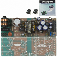
KIT DESIGN ACCELERATOR MODEM
Manufacturer
Power Integrations
Type
Design Accelerator Kit (DAK)r
Specifications of DAK-18
Contents
Power Supply, Samples, PCB, Software and Documentation
For Use With/related Products
TOP234P
Lead Free Status / RoHS Status
Not applicable / Not applicable
Other names
596-1002


05-Dec-2002
10 W, Multiple Output, Isolated Power Supply
recovery spike and damp the subsequent oscillations which might allow the drain to ring
below source at low line.
The bias winding is rectified and filtered by D6 and C11 to power U1. Capacitor C3 is
used to decouple the CONTROL pin, determine the auto-restart frequency and together
with R4, forms part of the control loop compensation.
The secondary winding is rectified and filtered by D7, R5, C4 (30 V) D8, C5 (5 V) and D9,
C7, C8 (3.3 V), with additional switching frequency ripple and high frequency spike noise
filtering provided by L2, C8 (5 V) and L3, C9 (3.3 V) to give the DC outputs.
The choice of Schottky diodes for the 3.3 V and 5 V outputs was driven by both voltage
regulation and efficiency considerations. Resistor R5 limits the diode current at start-up
and avoids peak charging of the 30 V output. If a fusible resistor is used, R5 can provide
short circuit protection for this output.
The snubber (C13 and R8) reduces the 10 MHz to 30 MHz conducted EMI due
secondary leakage inductance. The current through the pre-load resistor R13 adds to the
spec minimum load to keep the 30 V output in regulation. The 3.3 V and 5 V output
voltages are determined by the voltage set at the adjust pin of U3 (shunt regulator) by the
voltage divider formed by R10, R11 and R12. The current through R12 (250 µA) sets the
output voltages, while the current contribution of R10 and R11 (250 µA total) sets the
regulation band for 3.3 V and 5 V outputs, respectively. Other output voltages are
possible by adjusting the transformer turns ratios, choosing the output diodes forward
voltage drops and voltage divider settings. Optocoupler U2 applies the feedback signal
from U3 to the CONTROL pin of U1. Resistor R6 is used to set the overall gain of the
supply control loop, while R7 provides bias current for U3. Capacitor C10 provides
frequency compensation for U3 stabilizing the power supply control loop. Capacitor C14
is used to close the feedback loop (bypassing U3) through optocoupler U2 during start-
up, before U3 takes over the control loop. The ability to close the feedback loop in
conjunction with the built-in soft-start feature of TOPSwitch-GX completely controls the
start-up drain current profile, preventing transformer saturation and output overshoot.
The 3.3 V and 5 V secondary layout switching loops are minimized and, along with
closely coupled transformer secondary windings, achieve low secondary leakage
inductance and in turn, good cross-regulation. Optimizing the number of primary turns
minimizes leakage.
This also reduces the number of primary layers and improves
primary to secondary coupling.
The power supply meets IEC60950/UL1950 safety requirements. Primary-to-secondary
isolation is assured by using parts/materials (opto/transformer insulation) with the correct
level of isolation and creepage distances (opto slot/transformer bobbin).
The power supply passed IEC/UL 1000-4-5, Class 4 line surge test (Class 3 only is
required). All three outputs had monitor LEDs that showed no output disruption during
the 90 high voltage surge pulses of Class 3. During Class 4 testing the outputs were
Page 7 of 28
Power Integrations, Inc.
Tel: +1 408 414 9200 Fax: +1 408 414 9201
www.powerint.com
Related parts for DAK-18
Image
Part Number
Description
Manufacturer
Datasheet
Request
R

Part Number:
Description:
KIT REF DES DPA 6.6W DC-DC CONV
Manufacturer:
Power Integrations
Datasheet:

Part Number:
Description:
KIT DESIGN ACCELERATOR POE CONV
Manufacturer:
Power Integrations
Datasheet:

Part Number:
Description:
DESIGN ACCELERATOR KIT XT SWITCH
Manufacturer:
Power Integrations
Datasheet:

Part Number:
Description:
DESIGN ACCELERATOR KIT LP SWITCH
Manufacturer:
Power Integrations
Datasheet:

Part Number:
Description:
KIT DESIGN ACC PEAKSWITCH FAMILY
Manufacturer:
Power Integrations
Datasheet:

Part Number:
Description:
KIT DESIGN ACCELERATOR ADAPTER
Manufacturer:
Power Integrations
Datasheet:

Part Number:
Description:
KIT DESIGN ACCELERATOR ADAPTER
Manufacturer:
Power Integrations
Datasheet:

Part Number:
Description:
KIT DESIGN ACCELERATOR DC-DC
Manufacturer:
Power Integrations
Datasheet:

Part Number:
Description:
KIT DESIGN ACCELERATOR DPA SW
Manufacturer:
Power Integrations
Datasheet:

Part Number:
Description:
KIT DESIGN ACCELERATOR AC/DC PS
Manufacturer:
Power Integrations
Datasheet: