DAK-18 Power Integrations, DAK-18 Datasheet - Page 6
DAK-18
Manufacturer Part Number
DAK-18
Description
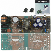
KIT DESIGN ACCELERATOR MODEM
Manufacturer
Power Integrations
Type
Design Accelerator Kit (DAK)r
Specifications of DAK-18
Contents
Power Supply, Samples, PCB, Software and Documentation
For Use With/related Products
TOP234P
Lead Free Status / RoHS Status
Not applicable / Not applicable
Other names
596-1002


10 W, Multiple Output, Isolated Power Supply
4 Circuit Description
The EP-18 is a low-cost flyback switching power supply designed for high speed digital
modem applications using the TOP243P integrated circuit. It offers a low cost solution
with emphasis on low EMI and ultra-low earth leakage current (no Y cap).
The circuit schematic details a 10 W, 3 output (3.3 VDC, 5 VDC and 30 VDC) power
supply that operates from an 85 VAC to 265 VAC input. The high efficiency (>70%)
allows the power supply to operate within specifications at elevated ambient temperature.
The AC input is rectified and filtered by D1 to D4 and C1 to create a high voltage DC bus
that is connected to transformer T1. The other side of T1 is driven by the high-voltage
MOSFET of TOP243P
failures,
overloaded/shorted outputs.
The combined value of the line sensing resistors R2 and R3, connected to the MULTI-
FUNCTION (M) pin of U1, sets the undervoltage and overvoltage thresholds and
provides a line feed forward function.
On increasing line voltage, the power supply is inhibited until the undervoltage (UV)
threshold is reached (~100 VDC). On reducing line voltage, the UV function turns off the
power supply when the line input voltage is below the UV threshold and the output goes
out of regulation. This allows the power supply to continue operating at input voltages
significantly below the UV threshold until output regulation is lost, but eliminates output
glitches by preventing restart until the input voltage goes back above the UV threshold.
The overvoltage function turns off the power supply if the input voltage exceeds
approximately 450 V.
transients or extended line swell conditions without damage. The supply resumes
operation when the input voltage falls below the overvoltage threshold.
The line feed forward function independently modulates the duty cycle of U1 to reject the
AC line frequency ripple component of the input voltage, reducing the line frequency
ripple at the output of the supply. The output ripple specifications can be met without
increased control loop gain since line feed forward operates independent of the main
control loop. This simplifies the design of the power supply control loop.
A low cost RCD (R1, C2, R9 and D5) snubber circuit limits the turn-off voltage spike
(caused by the leakage inductance) to a safe level on the DRAIN pin of U1. Resistor R9
is required in series with the slow recovery diode (D5) to reduce the diode reverse
1
pin. “Y” and “R” packages allow both functions via the L and X pins. Reducing the current limit in this
design would allow a smaller transformer to be used, if desired.
The “P” and “G” packages allow either line sensing or external current limit programming through the M
Power Integrations, Inc.
Tel: +1 408 414 9200 Fax: +1 408 414 9201
www.powerint.com
while
U1
1
protects
In the off-state, the power supply can withstand severe line
(U1).
Fuse F1 protects against primary-side components
against
secondary
components
failures,
05-Dec-2002
Page 6 of 28
and
Related parts for DAK-18
Image
Part Number
Description
Manufacturer
Datasheet
Request
R

Part Number:
Description:
KIT REF DES DPA 6.6W DC-DC CONV
Manufacturer:
Power Integrations
Datasheet:

Part Number:
Description:
KIT DESIGN ACCELERATOR POE CONV
Manufacturer:
Power Integrations
Datasheet:

Part Number:
Description:
DESIGN ACCELERATOR KIT XT SWITCH
Manufacturer:
Power Integrations
Datasheet:

Part Number:
Description:
DESIGN ACCELERATOR KIT LP SWITCH
Manufacturer:
Power Integrations
Datasheet:

Part Number:
Description:
KIT DESIGN ACC PEAKSWITCH FAMILY
Manufacturer:
Power Integrations
Datasheet:

Part Number:
Description:
KIT DESIGN ACCELERATOR ADAPTER
Manufacturer:
Power Integrations
Datasheet:

Part Number:
Description:
KIT DESIGN ACCELERATOR ADAPTER
Manufacturer:
Power Integrations
Datasheet:

Part Number:
Description:
KIT DESIGN ACCELERATOR DC-DC
Manufacturer:
Power Integrations
Datasheet:

Part Number:
Description:
KIT DESIGN ACCELERATOR DPA SW
Manufacturer:
Power Integrations
Datasheet:

Part Number:
Description:
KIT DESIGN ACCELERATOR AC/DC PS
Manufacturer:
Power Integrations
Datasheet: