KIT3468MMA7455L Freescale Semiconductor, KIT3468MMA7455L Datasheet - Page 18
KIT3468MMA7455L
Manufacturer Part Number
KIT3468MMA7455L
Description
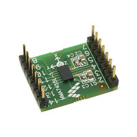
KIT EVALUATION FOR MMA7456L
Manufacturer
Freescale Semiconductor
Datasheet
1.RD3172MMA7455L.pdf
(35 pages)
Specifications of KIT3468MMA7455L
Sensor Type
Accelerometer, 3 Axis
Sensing Range
±2g, 4g, 8g
Interface
I²C, SPI
Sensitivity
16, 32, 64 LSB/g
Voltage - Supply
2.4 V ~ 3.6 V
Embedded
No
Utilized Ic / Part
MMA7455
Acceleration
2 g, 4 g, 6 g
Sensing Axis
Triple Axis
Output Type
Digital
Operating Voltage
3.6 V
Operating Current
400 uA
Maximum Operating Temperature
+ 85 C
Minimum Operating Temperature
- 40 C
Lead Free Status / RoHS Status
Lead free / RoHS Compliant
Available stocks
Company
Part Number
Manufacturer
Quantity
Price
Company:

Part Number:
KIT3468MMA7455L
Manufacturer:
Freescale Semiconductor
Quantity:
135


SPI Slave Interface
The MMA7455L also uses serial peripheral interface communication as a digital communication. The SPI communication is pri-
marily used for synchronous serial communication between a master device and one or more slave devices. See
an example of how to configure one master with one MMA745xL device. The MMA7455L is always operated as a slave device.
Typically, the master device would be a microcontroller which would drive the clock (SPC) and chip select (CS) signals.
The SPI interface consists of two control lines and two data lines: CS, SPC, SDI, and SDO. The CS, also known as Chip Select,
is the slave device enable which is controlled by the SPI master. CS is driven low at the start of a transmission. CS is then driven
high at the end of a transmission. SPC is the Serial Port Clock which is also controlled by the SPI master. SDI and SDO are the
Serial Port Data Input and the Serial Port Data Output. The SDI and SDO data lines are driven at the falling edge of the SPC and
should be captured at the rising edge of the SPC.
Read and write register commands are completed in 16 clock pulses or in multiples of 8, in the case of a multiple byte read/write.
SPI Read Operation
A SPI read transfer consists of a 1-bit Read/Write signal, a 6-bit address, and 1-bit don’t care bit. (1-bit R/W=0 + 6-bits address
+ 1-bit don’t care). The data to read is sent by the SPI interface during the next transfer. See
timing diagram for an 8-bit read in 4 wire and 3 wire modes, respectively.
SPI Write Operation
In order to write to one of the 8-bit registers, an 8-bit write command must be sent to the MMA7455L. The write command consists
of an MSB (0=read, 1=write) to indicate writing to the MMA7455L register, followed by a 6-bit address and 1 don’t care bit.
The command should then be followed the 8-bit data transfer. See
18
MMA7455L
Figure 11. SPI Timing Diagram for 8-Bit Register Read (4 Wire Mode)
Figure 12. SPI Timing Diagram for 8-Bit Register Read (3 Wire Mode)
Figure 13. SPI Timing Diagram for 8-Bit Register Write (3 Wire Mode)
Figure 13
for the timing diagram for an 8-bit data write.
Figure 11
Freescale Semiconductor
and
Figure 12
Figure 16
for the
Sensors
for
Related parts for KIT3468MMA7455L
Image
Part Number
Description
Manufacturer
Datasheet
Request
R

Part Number:
Description:
Manufacturer:
Freescale Semiconductor, Inc
Datasheet:
Part Number:
Description:
Manufacturer:
Freescale Semiconductor, Inc
Datasheet:
Part Number:
Description:
Manufacturer:
Freescale Semiconductor, Inc
Datasheet:
Part Number:
Description:
Manufacturer:
Freescale Semiconductor, Inc
Datasheet:
Part Number:
Description:
Manufacturer:
Freescale Semiconductor, Inc
Datasheet:
Part Number:
Description:
Manufacturer:
Freescale Semiconductor, Inc
Datasheet:
Part Number:
Description:
Manufacturer:
Freescale Semiconductor, Inc
Datasheet:
Part Number:
Description:
Manufacturer:
Freescale Semiconductor, Inc
Datasheet:
Part Number:
Description:
Manufacturer:
Freescale Semiconductor, Inc
Datasheet:
Part Number:
Description:
Manufacturer:
Freescale Semiconductor, Inc
Datasheet:
Part Number:
Description:
Manufacturer:
Freescale Semiconductor, Inc
Datasheet:
Part Number:
Description:
Manufacturer:
Freescale Semiconductor, Inc
Datasheet:
Part Number:
Description:
Manufacturer:
Freescale Semiconductor, Inc
Datasheet:
Part Number:
Description:
Manufacturer:
Freescale Semiconductor, Inc
Datasheet:
Part Number:
Description:
Manufacturer:
Freescale Semiconductor, Inc
Datasheet: