ADIS16365/PCBZ Analog Devices Inc, ADIS16365/PCBZ Datasheet - Page 4
ADIS16365/PCBZ
Manufacturer Part Number
ADIS16365/PCBZ
Description
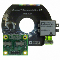
BOARD INTERFACE FOR ADIS16365
Manufacturer
Analog Devices Inc
Series
iMEMS®, iSensor™r
Specifications of ADIS16365/PCBZ
Sensor Type
Accelerometer, Gyroscope, 3 Axis
Sensing Range
±17g, ±75°/sec, ±150°/sec, ±300°/sec
Interface
SPI Serial
Sensitivity
3.3mg/LSB, 0.0125 ~ 0.05°/sec/LSB
Voltage - Supply
4.75 V ~ 5.25 V
Embedded
No
Utilized Ic / Part
ADIS16365
Silicon Manufacturer
Analog Devices
Application Sub Type
Accelerometer / Gyroscope
Kit Application Type
Sensing - Motion / Vibration / Shock
Silicon Core Number
ADIS16365
Lead Free Status / RoHS Status
Not applicable / RoHS Compliant
For Use With
ADISUSBZ - KIT EVAL ADIS W/SOFTWARE USB
Lead Free Status / RoHS Status
Lead free / RoHS Compliant, Not applicable / RoHS Compliant


ADIS16360/ADIS16365
Parameter
DAC OUTPUT
LOGIC INPUTS
DIGITAL OUTPUTS
FLASH MEMORY
FUNCTIONAL TIMES
CONVERSION RATE
POWER SUPPLY
1
2
3
4
5
The digital I/O signals are driven by an internal 3.3 V supply, and the inputs are 5 V tolerant.
Endurance is qualified as per JEDEC Standard 22, Method A117, and measured at −40°C, +25°C, +85°C, and +125°C.
The data retention lifetime equivalent is at a junction temperature (T
temperature.
These times do not include thermal settling and internal filter response times (330 Hz bandwidth), which may affect overall accuracy.
The sync input clock functions below the specified minimum value, at reduced performance levels.
Gain Error
Input Range
Input Capacitance
Resolution
Relative Accuracy
Differential Nonlinearity
Offset Error
Gain Error
Output Range
Output Impedance
Output Settling Time
Input High Voltage, V
Input Low Voltage, V
CS Wake-Up Pulse Width
Logic 1 Input Current, I
Logic 0 Input Current, I
Input Capacitance, C
Output High Voltage, V
Output Low Voltage, V
Data Retention
Power-On Start-Up Time
Reset Recovery Time
Sleep Mode Recovery Time
Flash Memory Test Time
Automatic Self-Test Time
Clock Accuracy
Sync Input Clock
Power Supply Current
All Pins Except RST
RST Pin
1
3
1
5
4
IL
IN
IH
OL
IH
IL
OH
Test Conditions/Comments
During acquisition
5 kΩ/100 pF to GND
101 LSB ≤ input code ≤ 4095 LSB
CS signal to wake up from sleep mode
V
V
I
I
Endurance
T
Time until data is available
Low power mode, SMPL_PRD ≥ 0x0A
Low power mode, SMPL_PRD ≥ 0x0A
Low power mode, SMPL_PRD ≥ 0x0A
Low power mode, SMPL_PRD ≥ 0x0A
SMPL_PRD = 0x0001 to 0x00FF
Operating voltage range, VCC
Low power mode
Normal mode
Sleep mode
Normal mode, SMPL_PRD ≤ 0x09
Normal mode, SMPL_PRD ≤ 0x09
Normal mode, SMPL_PRD ≤ 0x09
Normal mode, SMPL_PRD ≤ 0x09
SMPL_PRD = 0x0001
SOURCE
SINK
J
IH
IL
= 85°C
= 0 V
= 3.3 V
= 1.6 mA
= 1.6 mA
2
J
) of 85°C as per JEDEC Standard 22, Method A117. Data retention lifetime decreases with junction
Rev. D | Page 4 of 20
Min
0
0
2.0
20
2.4
10,000
20
0.413
0.8
4.75
Typ
±2
20
12
±4
±1
±5
±0.5
2
10
±0.2
40
1
10
180
250
60
130
4
9
17
90
12
5.0
24
49
500
Max
3.3
3.3
0.8
0.55
±10
60
0.4
819.2
±3
1.2
5.25
Unit
LSB
V
pF
Bits
LSB
LSB
mV
%
V
Ω
μs
V
V
V
μs
μA
μA
mA
pF
V
V
Cycles
Years
ms
ms
ms
ms
ms
ms
ms
ms
ms
SPS
%
kHz
V
mA
mA
μA
Related parts for ADIS16365/PCBZ
Image
Part Number
Description
Manufacturer
Datasheet
Request
R

Part Number:
Description:
±1.7g Dual-Axis IMEMS Accelerometer Evaluation Board
Manufacturer:
Analog Devices Inc
Datasheet:

Part Number:
Description:
Inertial Sensor Evaluation System
Manufacturer:
Analog Devices Inc
Datasheet:
Part Number:
Description:
Manufacturer:
Analog Devices Inc
Datasheet:
Part Number:
Description:
Manufacturer:
Analog Devices Inc
Datasheet:
Part Number:
Description:
Manufacturer:
Analog Devices Inc
Datasheet:
Part Number:
Description:
Manufacturer:
Analog Devices Inc
Datasheet:
Part Number:
Description:
Manufacturer:
Analog Devices Inc
Datasheet:
Part Number:
Description:
Manufacturer:
Analog Devices Inc
Datasheet:
Part Number:
Description:
Manufacturer:
Analog Devices Inc
Datasheet:
Part Number:
Description:
Manufacturer:
Analog Devices Inc
Datasheet:
Part Number:
Description:
Manufacturer:
Analog Devices Inc
Datasheet:
Part Number:
Description:
Manufacturer:
Analog Devices Inc
Datasheet:
Part Number:
Description:
Manufacturer:
Analog Devices Inc
Datasheet: