STEVAL-ISA056V1 STMicroelectronics, STEVAL-ISA056V1 Datasheet
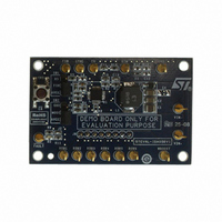
STEVAL-ISA056V1
Specifications of STEVAL-ISA056V1
Available stocks


Related parts for STEVAL-ISA056V1


STEVAL-ISA056V1 Summary of contents
Page 1
Features ■ Boost section – 4 input voltage range – Internal power MOSFET – Internal +5 V LDO for device supply – output voltage – Constant frequency peak current-mode control – 200 ...
Page 2
Contents Contents 1 Typical application circuit . . . . . . . . . . . . . . . . . . . . . . . . . . . . . . . . . . ...
Page 3
PM6600 9 Fault management . . . . . . . . . . . . . . . . . . . . . . . . . . . . . . . . . . . . ...
Page 4
Contents Appendix C Application suggestions . . . . . . . . . . . . . . . . . . . . . . . . . . . . . . . . . . 55 ...
Page 5
PM6600 List of figures Figure 1. Application circuit . . . . . . . . . . . . . . . . . . . . . . . . . . . . . . . . ...
Page 6
List of figures Figure 49. Main loop and current loop diagram . . . . . . . . . . . . . . . . . . . . . . . . . . . . . ...
Page 7
PM6600 1 Typical application circuit Figure 1. Application circuit LX 19 BILIM VIN 8 RILIM SYNC 23 Doc ID 14248 Rev 7 Typical application circuit SGND FSW 4 7/60 ...
Page 8
Pin settings 2 Pin settings 2.1 Connections Figure 2. Pin connection (through top view) 2.2 Pin description Table 2. Pin functions N° Pin 1 COMP 2 RILIM 3 BILIM 4 FSW 5 MODE 6 AVCC 7 LDO5 8 VIN 8/60 ...
Page 9
PM6600 Table 2. Pin functions (continued) N° Pin 9 SLOPE 10 SGND 11 ROW1 12 ROW2 13 ROW3 14 ROW4 15 ROW5 16 ROW6 17 PGND 18 OVSEL DIM FAULT 23 SYNC 24 SS ...
Page 10
Electrical data 3 Electrical data 3.1 Maximum rating Table 3. Absolute maximum ratings Symbol V AVCC to SGND AVCC V LDO5 to SGND LDO5 PGND to SGND V VIN to PGND SGND PGND ...
Page 11
PM6600 3.3 Recommended operating conditions Table 5. Recommended operating conditions Symbol Supply section V Input voltage range IN Boost section V Output voltage range BST Adjustable switching f SW frequency FSW sync input duty-cycle ROWs output maximum I rowx current ...
Page 12
Electrical characteristics 4 Electrical characteristics ° °C and MODE connected to AVCC unless specified IN A Table 6. Electrical characteristics Symbol Parameter Supply section V V LDO output and IC supply ...
Page 13
PM6600 Table 6. Electrical characteristics (continued) Symbol Parameter Boost section Minimum switching t on,min on time Default switching frequency Minimum FSW Sync frequency FSW sync Input low level threshold FSW sync Input hysteresis FSW sync Min ON time SYNC output ...
Page 14
Electrical characteristics Table 6. Electrical characteristics (continued) Symbol Parameter Soft-start and power management EN, turn-on level threshold EN, turn-off level threshold DIM, high level threshold DIM, low level threshold EN, pull-up current SS, charge current SS, end-of-startup threshold SS, reduced ...
Page 15
PM6600 5 Typical operating characteristics All the measures are done with a standard PM6600EVAL demonstration board and a standard WLED6021NB tamboured, with the components listed in the EVAL_KIT document. The measures are done with this working conditions, unless specified: ● ...
Page 16
Typical operating characteristics Figure 7. Efficiency vs DIM duty cycle @ f 100 DIM duty cycle [%] Figure 9. Efficiency vs DIM duty cycle @ Vin = ...
Page 17
PM6600 Figure 13. Efficiency vs Vin @ DIM duty cycles = 10% 100 Vin [V] Figure 15. Efficiency vs Vin @ DIM duty cycles = 75 ...
Page 18
Typical operating characteristics Figure 17. Working waveforms @ f = 100 Hz DIM Figure 19. Working waveforms @ f = 100 Hz 50% DIM 18/60 Figure 18. Working waveforms @ f = 100 Hz, D ...
Page 19
PM6600 Figure 21. Working waveforms @ f = 200 Hz DIM Figure 23. Working waveforms @ f = 200 Hz 50% DIM Typical operating characteristics Figure 22. Working waveforms @ f = 200 Hz, D ...
Page 20
Typical operating characteristics Figure 25. Working waveforms @ f = 500 Hz DIM Figure 27. Working waveforms @ kHz DIM 20/60 Figure 26. Working waveforms @ f = 500 Hz, D ...
Page 21
PM6600 Figure 29. Working waveforms @ kHz DIM Figure 31. Working waveforms @ kHz DIM Typical operating characteristics Figure 30. Working waveforms @ kHz, D ...
Page 22
Typical operating characteristics Figure 33. Output voltage ripple @ f = 200 Hz DIM Figure 35. Output voltage ripple @ f = 200 Hz 50% DIM 22/60 Figure 34. Output voltage ripple @ f = ...
Page 23
PM6600 Figure 37. Shorted LED protection @ f = 200 Hz DIM all WLEDs connected Figure 39. Shorted LED protection @ f = 200 Hz DIM 2 WLEDs shorted Typical operating characteristics Figure 38. Shorted LED protection @ f DIM ...
Page 24
Typical operating characteristics Figure 41. Open ROW detection @ f = 200 Hz DIM 24/60 Doc ID 14248 Rev 7 PM6600 ...
Page 25
PM6600 6 Block diagram Figure 42. Simplified block diagram LDO5 COMP BILIM SS SYNC Ext Sync Detector FSW AVCC EN MODE FAULT DIM Shutdown VIN SLOPE Current Sense Ramp +5V ZCD Generator LDO + + + UVLO _ Control Detector ...
Page 26
Operation description 7 Operation description 7.1 Boost section 7.1.1 Functional description The PM6600 is a monolithic LEDs driver for the backlight of LCD panels and it consists of a boost converter and six PWM-dimmable current generators. The input voltage range ...
Page 27
PM6600 where the first term represents the highest total forward voltage drop over active ROWs and the second is the voltage drop across the leading generator (400 mV typ.). The device continues to monitor the voltage drop across all the ...
Page 28
Operation description Figure 44. OVP threshold setting 7.3 Switching frequency selection and synchronization The switching frequency of the boost converter can be set in the 200 kHz-1 MHz range by connecting the FSW pin to ground through a resistor. Calculation ...
Page 29
PM6600 The SYNC pin is a synchronization output and provides a 34% (typ.) duty-cycle clock when the PM6600 is used as master or a replica of the FSW pin when used as slave used to connect multiple devices ...
Page 30
Operation description 7.4 System stability The boost section of the PM6600 is a fixed frequency, peak current-mode converter. During normal operation, a minimum voltage selection circuit compares all the voltage drops across the active current generators and provides the minimum ...
Page 31
PM6600 Equation 9 Once the output capacitor has been chosen, the R Equation 10 Where G = 2.7 S and g M The C capacitor is determined to place the frequency of the compensation zero 5 COMP times lower than ...
Page 32
Operation description Figure 48. Load transient response measurement set- +5V 7.4.2 Slope compensation The constant frequency, peak current-mode topology has the advantage of very easy loop compensation with output ceramic capacitors (reduced cost and ...
Page 33
PM6600 The SLOPE pin allows to properly set the amount of slope compensation connecting a simple resistor R starts at 35% (typ.) of each switching period and its slope is given by the following equation: Equation 13 Where K , ...
Page 34
Operation description nominal value to permit to use inductors with lower saturation current value; the nominal switching frequency is restored after the SS pin voltage has crossed 0 this mode, the current runaway is avoided. Figure 51. Soft-start ...
Page 35
PM6600 7.6 Boost current limit The design of the external components, especially the inductor and the flywheel diode, must be optimized in terms of size relying on the programmable peak current limit. The PM6600 improves the reliability of the final ...
Page 36
Operation description Figure 52. f DIM 7.8 Thermal protection In order to avoid damage due to high junction temperature, a thermal shutdown protection is implemented. When the junction temperature rises above 150 °C (typ.), the device turns off both the ...
Page 37
PM6600 8 Backlight driver section 8.1 Current generators The PM6600 is a LEDs driver with six channels (ROWs); each ROW is able to drive multiple LEDs in series (max and to sink maximum current, ...
Page 38
Backlight driver section Equation 20 Due to the spread of the LEDs' forward voltage, the total drop across the LED's strings will be different. The device will manage the unconnected ROWs according to the MODE pin setting (see Table 8 ...
Page 39
PM6600 9 Fault management The main loop keeps the ROW having the lowest voltage drop regulated to about 400 mV. This value slightly depends on the voltage across the remaining active ROWs. After the soft- start sequence, all protections turn ...
Page 40
Fault management 9.3 Open LED fault In case a ROW is not connected or a LED fails open, the device has two different behaviors according to the MODE pin status. If the MODE pin is high (connected to AVCC), the ...
Page 41
PM6600 If the fault disappears after toggling the EN pin, it means that the connection is again on and the problem can be detected as a previous intermittent connection. If the fault persists also after toggling the EN pin, it ...
Page 42
Package mechanical data 10 Package mechanical data In order to meet environmental requirements, ST offers these devices in different grades of ® ECOPACK packages, depending on their level of environmental compliance. ECOPACK specifications, grade definitions and product status are available ...
Page 43
PM6600 Figure 53. VFQFPN-24 mechanical data Doc ID 14248 Rev 7 Package mechanical data 43/60 ...
Page 44
Layout guidelines Appendix A Layout guidelines A.1 Basic points: ● The device thermal pad is SGND. ● The device has 2 GND pins: SGND and PGND A.1.1 GNDs planes - 1 device If the pcb has 2 layers, the PGND ...
Page 45
PM6600 Take care not to design the LX switching copper area near the COMP network, in order to avoid cross-talking between the power switching signal and the compensation one. A very important thing is to keep the feedbacks (ROWs) and ...
Page 46
Layout guidelines Top layer of the standard PM6600 demonstration board A.7 While referring to the PM6600EVAL_EN demonstration board, the PGND and SGND connections are more than one. In this case the PGND and SGND areas are separated in the top ...
Page 47
PM6600 The following pictures are the Gerber files of the PM6600EVAL_EN board. Figure 55. Top side Figure 56. Bottom side Vias specs: diameter 0.8 mm, hole 0 Doc ID 14248 Rev 7 Layout guidelines 1.1 cm 47/60 ...
Page 48
Application note Appendix B Application note B.1 Inductor selection Being the PM6600 mostly dedicated to notebook backlighting, real-estate applications dictate severe constrain in selecting the optimal inductor. The inductor choice must take into account different parameters like conduction losses (DCR), ...
Page 49
PM6600 B.4 Design example In order to help the design of an application using the PM6600, in this section a simple step- by-step design example is provided. A typical application could be the LCD backlight in a 14.1” LCD panel ...
Page 50
Application note Equation 25 whereas R is: 0 Equation 26 and Equation 27 The output voltage in the above calculations is considered as the maximum value (LED with the maximum forward voltage connected to the leading generator): Equation 28 Figure ...
Page 51
PM6600 It is important to highlight that the inductor choice involves not only the value itself but the saturation current (higher than the boost current limit), the rated RMS current (the compliance with the saturation current might be not enough; ...
Page 52
Application note defining D as: 2 The worst case for the output voltage ripple is when input voltage is lower (V A simple way to select the C In order to affect as less as possible the current generators, it ...
Page 53
PM6600 V has to be chosen in the range OVP Equation 37 Where Equation 38 R can be chosen is in the order of hundreds of kilo-ohms to reduce the leakage current in 1 the resistor divider. For example, setting ...
Page 54
Application note B.4.9 Soft-start The SS duration is set connecting a capacitor between the SS pin and GND. The capacitor is thus charged with a constant 5 μA current, forcing the SS pin voltage to ramp up. The current limit ...
Page 55
PM6600 Appendix C Application suggestions C.1 Full application schematic Figure 58. Full application schematic FAU Ren 2 10 0kR ...
Page 56
Application suggestions C.2 EN, DIM path in production line Normally, in production line, the LCD modules are connected to testing machines with long wires. The VIN, EN and DIM signals are provided with automatic testing equipment, such as relays and/or ...
Page 57
PM6600 In case of the DIM pin, we suggest to use a function generator. In case of using a power supply preferable to use 3.3 V and the same RC filter as the EN pin. For what concerns ...
Page 58
Application suggestions C.5 Inductor choice The inductor selection should be done according to the datasheet guidelines. The choice of the inductor value is explained in the page 49 . Moreover, the inductor has to be properly dimensioned also according to ...
Page 59
PM6600 11 Revision history Table 12. Document revision history Date 07-Dec-2007 21-Jan-2008 07-Apr-2008 20-Oct-2008 12-Feb-2009 29-Jun-2009 18-Feb-2010 Revision 1 Initial release 2 Updated Table 4, Table 5 3 Updated Section 3.3 on page 11 Updated Section 3.3 on page 11 ...
Page 60
... Information in this document is provided solely in connection with ST products. STMicroelectronics NV and its subsidiaries (“ST”) reserve the right to make changes, corrections, modifications or improvements, to this document, and the products and services described herein at any time, without notice. All ST products are sold pursuant to ST’s terms and conditions of sale. ...