LM2594APDBCKGEVB ON Semiconductor, LM2594APDBCKGEVB Datasheet - Page 9
LM2594APDBCKGEVB
Manufacturer Part Number
LM2594APDBCKGEVB
Description
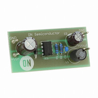
EVAL BOARD FOR LM2594APDBCKG
Manufacturer
ON Semiconductor
Specifications of LM2594APDBCKGEVB
Design Resources
LM2594APDBCKGEVB BOM LM2594APDBCKGEVB Schematic LM2594APDBCKGEVB Gerber Files
Main Purpose
DC/DC, Step Down
Outputs And Type
1, Non-Isolated
Voltage - Output
5V
Current - Output
500mA
Voltage - Input
4.5 ~ 40 V
Regulator Topology
Buck
Frequency - Switching
150kHz
Board Type
Fully Populated
Utilized Ic / Part
LM2594
Lead Free Status / RoHS Status
Lead free / RoHS Compliant
Power - Output
-
Lead Free Status / Rohs Status
Lead free / RoHS Compliant
For Use With/related Products
LM2594APDBCKG
Other names
LM2594ADPBCKGEVB
LM2594ADPBCKGEVBOS
LM2594APDBCKGEVBOS
LM2594ADPBCKGEVBOS
LM2594APDBCKGEVBOS


PROCEDURE (ADJUSTABLE OUTPUT VERSION: LM2594)
Given Parameters:
1. Programming Output Voltage
2. Input Capacitor Selection (C
3. Catch Diode Selection (D1)
V
V
I
To select the right programming resistor R1 and R2 value (see
Figure 1) use the following formula:
Resistor R1 can be between 1.0 k and 5.0 kW. (For best
temperature coefficient and stability with time, use 1% metal
film resistors).
To prevent large voltage transients from appearing at the input
and for stable operation of the converter, an aluminium or
tantalum electrolytic bypass capacitor is needed between the
input pin +V
located close to the IC using short leads. This capacitor should
have a low ESR (Equivalent Series Resistance) value.
For additional information see input capacitor section in the
“Application Information” section of this data sheet.
A. Since the diode maximum peak current exceeds the
B. The reverse voltage rating of the diode should be at least
Load(max)
out
in(max)
regulator maximum load current the catch diode current
rating must be at least 1.2 times greater than the maximum
load current. For a robust design, the diode should have a
current rating equal to the maximum current limit of the
LM2594 to be able to withstand a continuous output short.
1.25 times the maximum input voltage.
= Regulated Output Voltage
V out + V
= Maximum DC Input Voltage
= Maximum Load Current
in
and ground pin GND This capacitor should be
ref
R2 + R1
1.0 )
Procedure
R2
R1
in
V
V
)
out
ref
where V
* 1.0
ref
= 1.23 V
http://onsemi.com
9
Given Parameters:
1. Programming Output Voltage (selecting R1 and R2)
2. Input Capacitor Selection (C
the input and ground pin provides sufficient bypassing.
3. Catch Diode Selection (D1)
V
V
I
Select R1 and R2:
A 68 mF, 50 V aluminium electrolytic capacitor located near
A. For this example, a 1.0 A current rating is adequate.
B. For V
Load(max)
out
in(max)
R2 = 3.0 kW, choose a 3.0k metal film resistor.
any suggested fast recovery diode in the Table 2.
= 5.0 V
V out + 1.23 1.0 )
R2 + R1
= 12 V
in
= 0.5 A
= 12 V use a 20 V 1N5817 Schottky diode or
V out
V
ref
* 1.0
Example
R2
R1
in
)
+
Select R1 = 1.0 kW
1.23 V
5 V
* 1.0
Related parts for LM2594APDBCKGEVB
Image
Part Number
Description
Manufacturer
Datasheet
Request
R

Part Number:
Description:
ON Semiconductor [VOLTAGE REGULATOR]
Manufacturer:
ON Semiconductor
Datasheet:
Part Number:
Description:
357-036-542-201 CARDEDGE 36POS DL .156 BLK LOPRO
Manufacturer:
ON Semiconductor
Datasheet:
Part Number:
Description:
357-036-542-201 CARDEDGE 36POS DL .156 BLK LOPRO
Manufacturer:
ON Semiconductor
Datasheet:
Part Number:
Description:
357-036-542-201 CARDEDGE 36POS DL .156 BLK LOPRO
Manufacturer:
ON Semiconductor
Datasheet:
Part Number:
Description:
357-036-542-201 CARDEDGE 36POS DL .156 BLK LOPRO
Manufacturer:
ON Semiconductor
Datasheet:
Part Number:
Description:
357-036-542-201 CARDEDGE 36POS DL .156 BLK LOPRO
Manufacturer:
ON Semiconductor
Datasheet:
Part Number:
Description:
357-036-542-201 CARDEDGE 36POS DL .156 BLK LOPRO
Manufacturer:
ON Semiconductor
Datasheet:
Part Number:
Description:
357-036-542-201 CARDEDGE 36POS DL .156 BLK LOPRO
Manufacturer:
ON Semiconductor
Datasheet:
Part Number:
Description:
357-036-542-201 CARDEDGE 36POS DL .156 BLK LOPRO
Manufacturer:
ON Semiconductor
Datasheet:
Part Number:
Description:
357-036-542-201 CARDEDGE 36POS DL .156 BLK LOPRO
Manufacturer:
ON Semiconductor
Datasheet:
Part Number:
Description:
357-036-542-201 CARDEDGE 36POS DL .156 BLK LOPRO
Manufacturer:
ON Semiconductor
Datasheet:
Part Number:
Description:
Manufacturer:
ON Semiconductor
Datasheet:
Part Number:
Description:
Manufacturer:
ON Semiconductor
Datasheet:
Part Number:
Description:
Manufacturer:
ON Semiconductor
Datasheet: