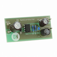
LM2594APDBCKGEVB ON Semiconductor, LM2594APDBCKGEVB Datasheet

LM2594APDBCKGEVB
Specifications of LM2594APDBCKGEVB
LM2594ADPBCKGEVBOS
LM2594APDBCKGEVBOS
Related parts for LM2594APDBCKGEVB
LM2594APDBCKGEVB Summary of contents
Page 1
LM2594 0.5 A, Step-Down Switching Regulator The LM2594 regulator is monolithic integrated circuit ideally suited for easy and convenient design of a step−down switching regulator (buck converter capable of driving a 0.5 A load with excellent line and ...
Page 2
V Unregulated +V DC Input PIN FUNCTION DESCRIPTION Pin No. Symbol 1 − Not Connected 4 FB This pin is the direct input of the error amplifier and the resistor ...
Page 3
MAXIMUM RATINGS Symbol V Maximum Supply Voltage in ON/OFF ON/OFF Pin Input Voltage V Output Voltage to Ground (Steady−State) out Power Dissipation P 8−Lead DIP D R Thermal Resistance, Junction−to−Ambient qJA R Thermal Resistance, Junction−to−Case qJC Power Dissipation P 8−Lead ...
Page 4
SYSTEM PARAMETERS ELECTRICAL CHARACTERISTICS over full Operating Temperature Range −40°C to +125°C Characteristics LM2594 (Note 1, Test Circuit Figure 16) Feedback Voltage ( 0 Load Feedback Voltage (8.0 V ≤ V ≤ ...
Page 5
TYPICAL PERFORMANCE CHARACTERISTICS 1 0 100 mA Load 0.6 Normalized 25°C J 0.4 0.2 0 -0.2 -0.4 -0.6 -0.8 -1.0 −50 − JUNCTION TEMPERATURE (°C) ...
Page 6
TYPICAL PERFORMANCE CHARACTERISTICS 1.3 1.2 1.1 1.0 −40°C 0.9 0.8 25°C 0.7 125°C 0.6 0.5 0.4 0.3 0 0.1 0.2 0.3 SWITCH CURRENT (A) Figure 9. Switch Saturation Voltage 5.0 4.5 4.0 3.5 3.0 2.5 2 ...
Page 7
TYPICAL PERFORMANCE CHARACTERISTICS ms/div Figure 14. Switching Waveforms out A: Output Pin Voltage, 10 V/div B: Switch Current, ...
Page 8
As in any switching regulator, the layout of the printed circuit board is very important. Rapidly switching currents associated with wiring inductance, stray capacitance and parasitic inductance of the printed circuit board traces can generate voltage transients which electromagnetic interferences ...
Page 9
PROCEDURE (ADJUSTABLE OUTPUT VERSION: LM2594) Procedure Given Parameters Regulated Output Voltage out V = Maximum DC Input Voltage in(max Maximum Load Current Load(max) 1. Programming Output Voltage To select the right programming resistor R1 and R2 ...
Page 10
PROCEDURE (ADJUSTABLE OUTPUT VERSION: LM2594) (CONTINUED) Procedure 4. Inductor Selection (L1) A. Use the following formula to calculate the inductor Volt x microsecond [V x ms] constant: V OUT OUT SAT ...
Page 11
LM2594 Series Buck Regulator Design Procedures Table 1. RECOMMENDED VALUES OF THE OUTPUT CAPACITOR AND FEEDFORWARD CAPACITOR (I = 0.5 A) load V ( 1000/10/ 680/250 60 35 1000/10/ 680/150 60 26 1000/10/ 470/10/ 60 140 20 1000/10/ ...
Page 12
Table 2. DIODE SELECTION Surface Mouns Schottky MBRS140 All of these diodes are rated to at least 60 V. MURS120 30 V 10BQ040 10BF10 40 V 10MQ040 more MBRS160 10BQ050 10MQ060 MBRS1100 10MQ090 ...
Page 13
Table 3. INDUCTOR MANUFACTURERS PART NUMBERS Schott Through Inductance Current Hole (mH) (A) L1 220 0.18 67143910 L2 150 0.21 67143920 L3 100 0.26 67143930 L4 68 0.32 67143940 L5 47 0.37 67148310 L6 33 0.44 67148320 L7 22 0.60 ...
Page 14
EXTERNAL COMPONENTS Input Capacitor ( The Input Capacitor Should Have a Low ESR For stable operation of the switch mode converter a low ESR (Equivalent Series Resistance) aluminium or solid tantalum bypass capacitor is needed between the input ...
Page 15
Catch Diode Locate the Catch Diode Close to the LM2594 The LM2594 is a step−down buck converter; it requires a fast diode to provide a return path for the inductor current when the switch turns off. This diode must be ...
Page 16
A toroid, pot core or E−core (closed magnetic structure) should be used in such applications. Do Not Operate an Inductor Beyond its Maximum ...
Page 17
Since the current rating of the LM2594 is only 0.5 A, the total package power dissipation for this switcher is quite low, ranging from approximately 0 0.75 W under varying conditions carefully engineered printed circuit ...
Page 18
V. This circuit configuration is able to deliver approximately 0. the output when the input ...
Page 19
100 Shutdown Input 5.0 V Off 470 MOC8101 NOTE: This picture does not show the complete circuit. Figure 25. Inverting Buck−Boost Regulator Shutdown Circuit Using an Optocoupler With ...
Page 20
Delayed Startup There are some applications, like the inverting regulator already mentioned above, which require a higher amount of startup current. In such cases, if the input power source is limited, this delayed startup feature becomes very useful. To provide ...
Page 21
V Max Unregulated DC Input +V in LM2594 GND 5 ON/OFF 100 mF Figure 31 Adjustable 0.5 A Power Supply with Low Output Ripple Feedback 4 L1 100 mH Output 8 ...
Page 22
THE LM2594 STEP−DOWN VOLTAGE REGULATOR WITH 5 0.5 A OUTPUT POWER CAPABILITY. TYPICAL APPLICATION WITH THROUGH−HOLE PC BOARD LAYOUT Unregulated +V DC Input in LM2594 GND C1 100 ...
Page 23
ORDERING INFORMATION Device LM2594DADJG LM2594DADJR2G LM2594PADJG †For information on tape and reel specifications, including part orientation and tape sizes, please refer to our Tape and Reel Packaging Specifications Brochure, BRD8011/D. Device Marking Package LM2594 SOIC-8 (Pb Free) LM2594 SOIC-8 (Pb ...
Page 24
... G C SEATING PLANE −Z− 0.25 (0.010 *For additional information on our Pb−Free strategy and soldering details, please download the ON Semiconductor Soldering and Mounting Techniques Reference Manual, SOLDERRM/D. PACKAGE DIMENSIONS SOIC−8 NB CASE 751−07 ISSUE 0.10 (0.004 SOLDERING FOOTPRINT* 1 ...
Page 25
... Equal Opportunity/Affirmative Action Employer. This literature is subject to all applicable copyright laws and is not for resale in any manner. PUBLICATION ORDERING INFORMATION LITERATURE FULFILLMENT: Literature Distribution Center for ON Semiconductor P.O. Box 5163, Denver, Colorado 80217 USA Phone: 303−675−2175 or 800−344−3860 Toll Free USA/Canada Fax: 303− ...


