STEVAL-ISA033V1 STMicroelectronics, STEVAL-ISA033V1 Datasheet - Page 11
STEVAL-ISA033V1
Manufacturer Part Number
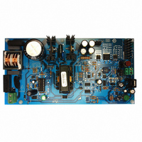
STEVAL-ISA033V1
Description
BOARD EVAL L5991/STP12NK80Z
Manufacturer
STMicroelectronics
Type
Supervisory Circuitsr
Specifications of STEVAL-ISA033V1
Main Purpose
AC/DC, Primary Side
Outputs And Type
3, Isolated
Power - Output
55W
Voltage - Output
13.8V, 3.8V, 25V
Current - Output
3A, 350mA, 200mA
Voltage - Input
88 ~ 300VAC
Regulator Topology
Flyback
Board Type
Fully Populated
Utilized Ic / Part
L5991, STP12NK80Z
Input Voltage
88 V to 300 V
Output Voltage
3.8 V to 25 V
Product
Power Management Modules
Lead Free Status / RoHS Status
Lead free / RoHS Compliant
Frequency - Switching
-
Lead Free Status / Rohs Status
Lead free / RoHS Compliant
For Use With/related Products
L5991, STP12NK80Z
Other names
497-8226
STEVAL-ISA033V1
STEVAL-ISA033V1
Available stocks
Company
Part Number
Manufacturer
Quantity
Price
Company:

Part Number:
STEVAL-ISA033V1
Manufacturer:
STMicroelectronics
Quantity:
1


Since the system tries restarting each hiccup cy-
cle, there is not any latchoff risk.
"Hiccup" keeps the system in control in case of
short circuits but does not eliminate power com-
ponents overstress during pulse-by-pulse limita-
tion (from A to C). Other external protection cir-
cuits are needed if a better control of overloads is
required.
Pin 8. VCC (Controller Supply). This pin supplies
the signal part of the IC. The device is enabled as
VCC voltage exceeds the start threshold and
works as long as the voltage is above the UVLO
threshold. Otherwise the device is shut down and
the
(<150 A). This is particularly useful for reducing
the consumption of the start-up circuit (in the sim-
plest case, just one resistor), which is one of the
most significant contributions to power losses in
standby.
An internal Zener limits the voltage on VCC to
25V. The IC current consumption increases con-
siderably if this limit is exceeded.
A small film capacitor between this pin and SGND
(pin 12), placed as close as possible to the IC, is
recommended to filter high frequency noise.
Pin 9. VC (Supply of the Power Stage). It supplies
the driver of the external switch and therefore ab-
sorbs a pulsed current. Thus it is recommended to
place a buffer capacitor (towards PGND, pin 11,
as close as possible to the IC) able to sustain
these current pulses and in order to avoid them
inducing disturbances.
This pin can be connected to the buffer capacitor
directly or through a resistor, as shown in fig. 27,
to control separately the turn-on and turn-off
speed of the external switch, typically a Power-
Figure 26. Hiccup mode operation.
FAULT
current
I
I
OUT
SEN
SS
0.5V
5V
consumption
is
extremely low
T
hic
SHORT
MOS. At turn-on the gate resistance is R
turn-off is R
Figure 27. Turn-on and turn-off speeds adjust-
Pin 10. OUT (Driver Output). This pin is the out-
put of the driver stage of the external power
switch. Usually, this will be a PowerMOS, al-
though the driver is powerful enough to drive
BJT’s (1.6A source, 2A sink, peak).
The driver is made up of a totem pole with a high-
side NPN Darlington and a low-side VDMOS, thus
there is no need of an external diode clamp to
prevent voltage from going below ground. An in-
ternal clamp limits the voltage delivered to the
gate at 13V. Thus it is possible to supply the
driver (Pin 9) with higher voltages without any risk
of damage for the gate oxide of the external MOS.
The clamp does not cause any additional in-
crease of power dissipation inside the chip since
the current peak of the gate charge occurs when
the gate voltage is few volts and the clamp is not
active. Besides, no current flows when the gate
voltage is 13V, steady state.
Under UVLO conditions an internal circuit (shown
CONTROL
DRIVE &
L5991
D97IN726
V
CC
13V
8
g
ment.
Rg'
PGND
only.
D98IN986
V
9
11
C
10
OUT
Rg
L5991 - L5991A
7V
Rg(ON)=Rg+Rg'
Rg(OFF)=Rg
g
time
+ R
11/23
g’
, at
Related parts for STEVAL-ISA033V1
Image
Part Number
Description
Manufacturer
Datasheet
Request
R

Part Number:
Description:
BOARD RGB CTR ST7,STP08C596MTR
Manufacturer:
STMicroelectronics
Datasheet:

Part Number:
Description:
Power Management IC Development Tools Full Speed USB to RS232 Bridge Demo
Manufacturer:
STMicroelectronics
Datasheet:
Part Number:
Description:
Power Management IC Development Tools 2.5W solar eval BRD USB SPV1040 LD39050
Manufacturer:
STMicroelectronics
Datasheet:

Part Number:
Description:
BOARD EVAL FOR MEMS SENSORS
Manufacturer:
STMicroelectronics
Datasheet:

Part Number:
Description:
KIT DEV STARTER ST10F276Z5
Manufacturer:
STMicroelectronics
Datasheet:

Part Number:
Description:
BOARD EVAL HDMI $ VIDEO SWITCH
Manufacturer:
STMicroelectronics
Datasheet:

Part Number:
Description:
BOARD DEMO ACCELEROMETER DIL24
Manufacturer:
STMicroelectronics
Datasheet:

Part Number:
Description:
BOARD STLM75/STDS75/ST72F651
Manufacturer:
STMicroelectronics
Datasheet:

Part Number:
Description:
EVAL BOARD 3AXIS MEMS ACCELLRMTR
Manufacturer:
STMicroelectronics
Datasheet:

Part Number:
Description:
BOARD EVAL 8BIT MICRO + TDE1708
Manufacturer:
STMicroelectronics
Datasheet:
Part Number:
Description:
STMicroelectronics [RIPPLE-CARRY BINARY COUNTER/DIVIDERS]
Manufacturer:
STMicroelectronics
Datasheet:
Part Number:
Description:
STMicroelectronics [LIQUID-CRYSTAL DISPLAY DRIVERS]
Manufacturer:
STMicroelectronics
Datasheet:
Part Number:
Description:
BOARD EVAL FOR MEMS SENSORS
Manufacturer:
STMicroelectronics
Datasheet: