STEVAL-ISA033V1 STMicroelectronics, STEVAL-ISA033V1 Datasheet
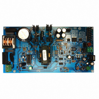
STEVAL-ISA033V1
Specifications of STEVAL-ISA033V1
STEVAL-ISA033V1
Available stocks


Related parts for STEVAL-ISA033V1


STEVAL-ISA033V1 Summary of contents
Page 1
N-channel 800V - 0.65Ω - 10.5A - TO-220 - D Zener - Protected SuperMESH™ Power MOSFET Features V DSS Type R DS(on) (@Tjmax) STB12NK80Z 800V <0.75Ω 10.5 A 190W STP12NK80Z 800V <0.75Ω 10.5 A 190W STW12NK80Z 800V <0.75Ω 10.5 A ...
Page 2
Contents Contents 1 Electrical ratings . . . . . . . . . . . . . . . . . . . . . . . . . . . . . . . . . . . ...
Page 3
STB12NK80Z - STP12NK80Z - STW12NK80Z 1 Electrical ratings Table 1. Absolute maximum ratings Symbol V Drain-source voltage ( Drain-gate voltage (R DGR V Gate-source voltage GS I Drain current (continuous Drain current (continuous) at ...
Page 4
Electrical characteristics 2 Electrical characteristics (T =25°C unless otherwise specified) CASE Table 4. On/off states Symbol Drain-source breakdown V (BR)DSS voltage Peak diode recovery I DSS voltage slope Gate body leakage current I GSS ( Gate ...
Page 5
STB12NK80Z - STP12NK80Z - STW12NK80Z Table 6. Source drain diode Symbol I Source-drain current SD (1) I Source-drain current (pulsed) SDM (2) V Forward on voltage SD t Reverse recovery time rr Q Reverse recovery charge rr I Reverse recovery ...
Page 6
Electrical characteristics 2.1 Electrical characteristics (curves) Figure 1. Safe operating area for TO-220/ D²PAK Figure 3. Safe operating area for TO-247 Figure 5. Output characteristics 6/16 STB12NK80Z - STP12NK80Z - STW12NK80Z Figure 2. Thermal impedance for TO-220/ D²PAK Figure 4. ...
Page 7
STB12NK80Z - STP12NK80Z - STW12NK80Z Figure 7. Transconductance Figure 9. Gate charge vs gate-source voltage Figure 10. Capacitance variations Figure 11. Normalized gate threshold voltage vs temperature Electrical characteristics Figure 8. Static drain-source on resistance Figure 12. Normalized on resistance ...
Page 8
Electrical characteristics Figure 13. Source-drain diode forward characteristics Figure 15. Maximum avalanche energy vs temperature 8/16 STB12NK80Z - STP12NK80Z - STW12NK80Z Figure 14. Normalized B VDSS vs temperature ...
Page 9
STB12NK80Z - STP12NK80Z - STW12NK80Z 3 Test circuit Package mechanical data Figure 16. Switching times test circuit for resistive load Figure 18. Test circuit for inductive load switching and diode recovery times Figure 20. Unclamped inductive waveform Test circuit Package ...
Page 10
Package mechanical data 4 Package mechanical data In order to meet environmental requirements, ST offers these devices in ECOPACK® packages. These packages have a Lead-free second level interconnect. The category of second level interconnect is marked on the package and ...
Page 11
STB12NK80Z - STP12NK80Z - STW12NK80Z Dim L20 L30 ∅P Q TO-220 mechanical data mm Min Typ Max 4.40 4.60 0.61 0.88 1.14 1.70 0.49 0.70 15.25 ...
Page 12
Package mechanical data DIM øP øR S 12/16 STB12NK80Z - STP12NK80Z - STW12NK80Z TO-247 MECHANICAL DATA mm. MIN. TYP MAX. 4.85 5.15 2.20 2.60 1.0 1.40 2.0 2.40 ...
Page 13
STB12NK80Z - STP12NK80Z - STW12NK80Z DIM PAK MECHANICAL DATA TO-247 MECHANICAL DATA mm. MIN. TYP MAX. 4.4 4.6 2.49 2.69 ...
Page 14
Packing mechanical data 5 Packing mechanical data 2 D PAK FOOTPRINT TAPE MECHANICAL DATA mm DIM. MIN. A0 10.5 B0 15.7 D 1.5 D1 1.59 E 1.65 F 11.4 K0 4.8 P0 3.9 P1 11 ...
Page 15
STB12NK80Z - STP12NK80Z - STW12NK80Z 6 Revision history Table 8. Revision history Date 22-Jun-2004 28-Jan-2005 08-Sep-2005 31-Jul-2006 27-Apr-2007 Revision 2 Preliminary version 3 Complete version 4 Figure 1 and Figure 3 5 The document has been reformatted 6 Modified Rds(on) ...
Page 16
... Information in this document is provided solely in connection with ST products. STMicroelectronics NV and its subsidiaries (“ST”) reserve the right to make changes, corrections, modifications or improvements, to this document, and the products and services described herein at any time, without notice. All ST products are sold pursuant to ST’s terms and conditions of sale. ...