STEVAL-ISA043V2 STMicroelectronics, STEVAL-ISA043V2 Datasheet - Page 6
STEVAL-ISA043V2
Manufacturer Part Number
STEVAL-ISA043V2
Description
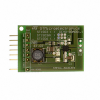
BOARD EVAL BASED ON ST1S06
Manufacturer
STMicroelectronics
Datasheets
1.ST1S06PUR.pdf
(20 pages)
2.STEVAL-ISA043V1.pdf
(4 pages)
3.STEVAL-ISA043V2.pdf
(12 pages)
Specifications of STEVAL-ISA043V2
Main Purpose
DC/DC, Step Down
Outputs And Type
1, Non-Isolated
Voltage - Output
3.3V
Current - Output
1.5A
Voltage - Input
2.7 ~ 6V
Regulator Topology
Buck
Frequency - Switching
1.5MHz
Board Type
Fully Populated
Utilized Ic / Part
ST1S06
Product
Power Management Modules
Silicon Manufacturer
ST Micro
Silicon Core Number
ST1S06PUR
Kit Application Type
Power Management - Voltage Regulator
Application Sub Type
Synchronous Buck Converter
Kit Contents
Board
Rohs Compliant
Yes
Lead Free Status / RoHS Status
Lead free / RoHS Compliant
Power - Output
-
Lead Free Status / Rohs Status
Lead free / RoHS Compliant
Other names
497-6420
STEVAL-ISA043V2
STEVAL-ISA043V2
Available stocks
Company
Part Number
Manufacturer
Quantity
Price
Company:

Part Number:
STEVAL-ISA043V2
Manufacturer:
STMicroelectronics
Quantity:
1


Thermal considerations
2
6/12
Thermal considerations
The dissipated power of the device is related to three different sources:
1.
Equation 7
Equation 8
2.
Equation 9
3.
Equation 10
Equation 11
The junction temperature of device will be:
Equation 12
Where T
ambient. Considering that the device in mounted on board with a good ground plane has a
thermal resistance junction to ambient (Rth
ambient temperature of about 85°C.
Equation 13
P
TOT
Switch losses due to the not negligible R
Where D is the duty cycle of the application. Note that the duty cycle is theoretically
given by the ratio between V
to compensate the losses of the overall application. Due to this reason, the switch
losses related to the R
Switch losses due to its turn-on and off. These are given by the following relation:
Where t
the current flowing into it during the turn-on and turn-off phases. t
switching time.
Quiescent current losses
Where I
R
0.16 Ω @ 150 °C. We can consider a value of 0.15 Ω . t
a typical value of 1.5 mA @ Vin = 5V. The overall losses are:
DS(on)
=
A
=
R
is the ambient temperature and Rth
DS on
0.15
ON
Q
has a typical value of 0.12 Ω @ 25 °C and increases up to a maximum value of
(
⋅
is the quiescent current. Example: V
P
and t
) P
1.5
SW
–
2
⋅
⋅
=
OFF
0.73
I
V
2
OUT
IN
+
are the overlap times of the voltage across the power switch and
⋅
0.12
DS(on)
⋅
I
P
OUT
D
⋅
ON P
P
+
1.5
T
ON P
R
–
⋅
J
OUT
DS on
2
T
increases compared with the ideal case.
(
------------------------------- -
⋅
–
=
J
=
t
(
ON
(
1 0.73
=
85
R
=
and V
–
) N
T
DS on
+
P
–
2
+
R
A
Q
t
OFF
DS on
(
0.552
+
⋅
)
=
J-A
+
Rth
in
(
) P
I
2
5
–
)
V
, but in practical is quite higher than this value
DS(on)
OUT
J-A
) of about 55 °C/W and considering an
⋅
⋅
IN
) P
J A
⋅
–
⋅
1.5
F
–
⋅
55
I
is the thermal resistance junction to
SW
⋅
⋅
2
⋅
I
OUT
⋅
IN
(
. These are equal to:
Q
=
I
20
1 D
2
=
P
–
OUT
115° C
= 5 V, V
⋅
TOT
V
⋅
10
)
IN
+
(
–
⋅
1 D
V
9
⋅
SW
IN
D
⋅
–
I
OUT
1.5
⋅
OUT
is approximately 20 ns. I
)
I
OUT
⋅
⋅
10
= 3.3 V, Iout = 1.5 A
t
6
⋅
SW
+
t
SW
5
SW
⋅
⋅
⋅
1.5
F
F
is the equivalent
SW
SW
⋅
10
+
–
V
3
IN
≅
0.552 W
⋅
AN2371
I
Q
Q
=
has
Related parts for STEVAL-ISA043V2
Image
Part Number
Description
Manufacturer
Datasheet
Request
R

Part Number:
Description:
BOARD RGB CTR ST7,STP08C596MTR
Manufacturer:
STMicroelectronics
Datasheet:

Part Number:
Description:
Power Management IC Development Tools Full Speed USB to RS232 Bridge Demo
Manufacturer:
STMicroelectronics
Datasheet:
Part Number:
Description:
Power Management IC Development Tools 2.5W solar eval BRD USB SPV1040 LD39050
Manufacturer:
STMicroelectronics
Datasheet:

Part Number:
Description:
BOARD EVAL FOR MEMS SENSORS
Manufacturer:
STMicroelectronics
Datasheet:

Part Number:
Description:
KIT DEV STARTER ST10F276Z5
Manufacturer:
STMicroelectronics
Datasheet:

Part Number:
Description:
BOARD EVAL HDMI $ VIDEO SWITCH
Manufacturer:
STMicroelectronics
Datasheet:

Part Number:
Description:
BOARD DEMO ACCELEROMETER DIL24
Manufacturer:
STMicroelectronics
Datasheet:

Part Number:
Description:
BOARD STLM75/STDS75/ST72F651
Manufacturer:
STMicroelectronics
Datasheet:

Part Number:
Description:
EVAL BOARD 3AXIS MEMS ACCELLRMTR
Manufacturer:
STMicroelectronics
Datasheet:

Part Number:
Description:
BOARD EVAL 8BIT MICRO + TDE1708
Manufacturer:
STMicroelectronics
Datasheet:
Part Number:
Description:
STMicroelectronics [RIPPLE-CARRY BINARY COUNTER/DIVIDERS]
Manufacturer:
STMicroelectronics
Datasheet:
Part Number:
Description:
STMicroelectronics [LIQUID-CRYSTAL DISPLAY DRIVERS]
Manufacturer:
STMicroelectronics
Datasheet:
Part Number:
Description:
BOARD EVAL FOR MEMS SENSORS
Manufacturer:
STMicroelectronics
Datasheet: