NCP1207AADAPGEVB ON Semiconductor, NCP1207AADAPGEVB Datasheet - Page 3
NCP1207AADAPGEVB
Manufacturer Part Number
NCP1207AADAPGEVB
Description
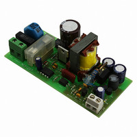
EVAL BOARD FOR NCP1207AADAPG
Manufacturer
ON Semiconductor
Datasheets
1.NCP1207APG.pdf
(17 pages)
2.NCP1207AADAPGEVB.pdf
(5 pages)
3.NCP1207AADAPGEVB.pdf
(8 pages)
Specifications of NCP1207AADAPGEVB
Design Resources
NCP1207AADAPGEVB BOM NCP1207AADAPGEVB Gerber Files NCP1207A EVB Schematic
Main Purpose
AC/DC, Primary Side
Outputs And Type
1, Isolated
Power - Output
24W
Voltage - Output
12V
Current - Output
2A
Voltage - Input
180 ~ 240VAC
Regulator Topology
Flyback
Frequency - Switching
70kHz
Board Type
Fully Populated
Utilized Ic / Part
NCP1207
Lead Free Status / RoHS Status
Lead free / RoHS Compliant
For Use With/related Products
NCP1207AADAPG
Other names
NCP1207AADAPGEVBOS


Stresses exceeding Maximum Ratings may damage the device. Maximum Ratings are stress ratings only. Functional operation above the
Recommended Operating Conditions is not implied. Extended exposure to stresses above the Recommended Operating Conditions may affect
device reliability.
MAXIMUM RATINGS
Power Supply Voltage, V
Transient Power Supply Voltage, Duration < 10 ms, I
Maximum Voltage on Pin 5 (Drv)
Maximum Voltage on all other pins except Pin 8 (HV), Pin 6 (V
Maximum Current for all pins except V
activated
Maximum Current in Pin 1
Thermal Resistance, Junction--to--Case
Thermal Resistance, Junction--to--Air, SOIC version
Thermal Resistance, Junction--to--Air, DIP8 version
Operating Junction Temperature
Maximum Junction Temperature
Temperature Shutdown
Hysteresis in Shutdown
Storage Temperature Range
ESD Capability, HBM Model (All pins except HV)
ESD Capability, Machine Model
Maximum Voltage on Pin 8 (HV), Pin 6 (V
Minimum Voltage on Pin 8 (HV), Pin 6 (V
GND
V
HV
CC
mA
7.0
*S and R are level triggered whereas S is edge
To Internal
triggered. R has priority over the other inputs.
Supply
5.3 V (fault)
12 V, 10 V,
+
--
CC
+
PON
Pin, Continuous Voltage
Mngt.
Fault
CC
5.0 V
CC
CC
(6), HV (8) and Demag (1) when 10 V ESD diodes are
) decoupled to ground with 10 mF
OVP
+
) decoupled to ground with 10 mF
Rating
Figure 2. Internal Circuit Architecture
--
/1.44
+
VCC
Demag
< 20 mA
http://onsemi.com
4.5/1.5ms
Delay
Timeout
CC
5.0 ms
Overload?
) and Pin 5 (Drv)
Blanking
3
8/4.5ms
R*
S*
S
VUVLO
R
Timeout
Q
Q
Reset
+
+
--
+
--
Soft--Start = 1 ms
50 mV
V
V
+
--
Symbol
V
CC
CC
V
TJ
Idem
R
HVMAX
R
R
HVMIN
T
1.0 V
θJC
θJA
θJA
MAX
Static
Pulse
--
--
--
--
--
--
--
--
J
Demag
+
V
CC
when Drv
380 ns
Driver: src = 20
L.E.B.
200 mA
is OFF
R
--40 to +125
--60 to +150
/3
--0.3 to 10
+3.0/--2.0
int
sink = 10
Value
178
100
150
155
200
500
5.0
2.0
20
25
20
57
30
40
R
10 V
4.2 V
esd
FB
CS
Demag
Drv
Units
C/W
C/W
C/W
mA
mA
C
C
C
C
C
kV
V
V
V
V
V
V
V
Related parts for NCP1207AADAPGEVB
Image
Part Number
Description
Manufacturer
Datasheet
Request
R

Part Number:
Description:
PWM Current-Mode Controller for Free Running Quasi-Resonant Operation
Manufacturer:
ON

Part Number:
Description:
ON Semiconductor [VOLTAGE REGULATOR]
Manufacturer:
ON Semiconductor
Datasheet:
Part Number:
Description:
357-036-542-201 CARDEDGE 36POS DL .156 BLK LOPRO
Manufacturer:
ON Semiconductor
Datasheet:
Part Number:
Description:
357-036-542-201 CARDEDGE 36POS DL .156 BLK LOPRO
Manufacturer:
ON Semiconductor
Datasheet:
Part Number:
Description:
357-036-542-201 CARDEDGE 36POS DL .156 BLK LOPRO
Manufacturer:
ON Semiconductor
Datasheet:
Part Number:
Description:
357-036-542-201 CARDEDGE 36POS DL .156 BLK LOPRO
Manufacturer:
ON Semiconductor
Datasheet:
Part Number:
Description:
357-036-542-201 CARDEDGE 36POS DL .156 BLK LOPRO
Manufacturer:
ON Semiconductor
Datasheet:
Part Number:
Description:
357-036-542-201 CARDEDGE 36POS DL .156 BLK LOPRO
Manufacturer:
ON Semiconductor
Datasheet:
Part Number:
Description:
357-036-542-201 CARDEDGE 36POS DL .156 BLK LOPRO
Manufacturer:
ON Semiconductor
Datasheet:
Part Number:
Description:
357-036-542-201 CARDEDGE 36POS DL .156 BLK LOPRO
Manufacturer:
ON Semiconductor
Datasheet:
Part Number:
Description:
357-036-542-201 CARDEDGE 36POS DL .156 BLK LOPRO
Manufacturer:
ON Semiconductor
Datasheet:
Part Number:
Description:
357-036-542-201 CARDEDGE 36POS DL .156 BLK LOPRO
Manufacturer:
ON Semiconductor
Datasheet:
Part Number:
Description:
Manufacturer:
ON Semiconductor
Datasheet:
Part Number:
Description:
Manufacturer:
ON Semiconductor
Datasheet: