LM20144EVAL National Semiconductor, LM20144EVAL Datasheet - Page 4
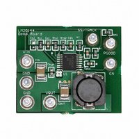
LM20144EVAL
Manufacturer Part Number
LM20144EVAL
Description
BOARD EVAL 4A POWERWISE LM20144
Manufacturer
National Semiconductor
Series
PowerWise®r
Specifications of LM20144EVAL
Main Purpose
DC/DC, Step Down
Outputs And Type
1, Non-Isolated
Voltage - Output
1.2V
Current - Output
4A
Voltage - Input
2.95 ~ 5.5V
Regulator Topology
Buck
Frequency - Switching
1MHz
Board Type
Fully Populated
Utilized Ic / Part
LM20144
Lead Free Status / RoHS Status
Not applicable / Not applicable
Power - Output
-


www.national.com
Component Selection
This section provides a walk-through of the design process of
the LM20144 evaluation board. Unless otherwise indicated all
equations assume units of Amps (A) for current, Farads (F)
for capacitance, Henries (H) for inductance, and Volts (V) for
voltages.
INPUT CAPACITOR
The required RMS current rating of the input capacitor for a
buck regulator can be estimated by the following equation:
The variable D refers to the duty cycle, and can be approxi-
mated by:
From this equation, it follows that the maximum I
quirement will occur at a full 4A load current with the system
operating at 50% duty cycle. Under this condition, the maxi-
mum I
Ceramic capacitors feature a very large I
footprint, making a ceramic capacitor ideal for this application.
A 100 µF X5R ceramic capacitor from Murata with a 5.4A
I
evaluation board. For improved bypassing, a small 1 µF high
frequency capacitor is placed in parallel with the 100 µF bulk
capacitor to filter high frequency noise pulses on the supply.
AVIN FILTER
An RC filter should be added to prevent any switching noise
on PVIN from interfering with the internal analog circuitry con-
nected to AVIN. These can be seen on the schematic as
components R
of the resistor R
of current during startup, and if R
voltage drop can trigger the UVLO comparator. For the demo
board a 1Ω resistor is used for R
be triggered after the part is enabled. A recommended 1 µF
C
16dB of attenuation at a 1MHz switching frequency.
INDUCTOR
As per the datasheet recommendations, the inductor value
should initially be chosen to give a peak to peak ripple current
equal to roughly 30% of the maximum output current. The
peak to peak inductor ripple current can be calculated by the
equation:
Rearranging this equation and solving for the inductance re-
veals that for this application (V
MHz, and I
0.76 µH. Rounding up to the nearest standard inductor value,
a final inductance of 1 µH is selected. This results in a peak-
RMS
F
capacitor coupled with the 1Ω resistor provides roughly
rating provides the necessary input capacitance for the
CIN(RMS)
OUT
is given by:
F
= 4A) the nominal inductance value is roughly
F
and C
as the AVIN pin will draw a short 60mA burst
F
. There is a practical limit to the size
IN
F
ensuring that UVLO will not
= 5V, V
F
is too large the resulting
RMS
OUT
rating in a small
= 1.2V, f
CIN(RMS)
SW
= 1
re-
4
to-peak ripple current of 912 mA and 1.122A when the con-
verter is operating from 5V and 3.3V respectively. Once an
inductance value is calculated, an actual inductor needs to be
selected based on a trade-off between physical size, efficien-
cy, and current carrying capability. For the LM20144 evalua-
tion board, a Coilcraft MSS1038-102NL inductor offers a good
balance between efficiency (6 mΩ DCR), size, and saturation
current rating (9A I
OUTPUT CAPACITOR
The value of the output capacitor in a buck regulator influ-
ences the voltage ripple that will be present on the output
voltage, as well as the large signal output voltage response
to a load transient. Given the peak-to-peak inductor current
ripple (ΔI
by the equation:
The variable R
pacitor. As can be seen in the above equation, the ripple
voltage on the output can be divided into two parts, one of
which is attributed to the AC ripple current flowing through the
ESR of the output capacitor and another due to the AC ripple
current actually charging and discharging the output capaci-
tor. The output capacitor also has an effect on the amount of
droop that is seen on the output voltage in response to a load
transient event.
For the evaluation board, a Murata 100 µF ceramic capacitor
is selected for the output capacitor to provide good transient
and DC performance in a relatively small package. From the
technical specifications of this capacitor, the ESR is roughly
2 mΩ, and the effective in-circuit capacitance is approximate-
ly 55 µF (reduced from 100 µF due to the 1.2V DC bias). With
these values, the peak to peak voltage ripple on the output
when operating from a 5V input can be calculated to be 3.9
mV.
C
A soft-start capacitor can be used to control the startup time
of the LM20144 voltage regulator. The startup time of the
regulator when using a soft-start capacitor can be estimated
by the following equation:
For the LM20144, I
board, the soft-start time has been designed to be roughly 5
ms, resulting in a C
C
The C
subregulator. This capacitor should be sized equal to or
greater than 1 µF, but less than 10 µF. A value of 1 µF is
sufficient for most applications.
C
The capacitor C
the LM20144 control loop. Since this board was optimized to
work well over the full input and output voltage range, the val-
ue of C
conditions for the device are known, the transient response
SS
VCC
C1
VCC
C1
P-P
capacitor is necessary to bypass an internal 2.7V
was selected to be 3.3 nF. Once the operating
) the output voltage ripple can be approximated
ESR
C1
SAT
above refers to the ESR of the output ca-
is used to set the crossover frequency of
SS
SS
capacitor value of 33 nF.
rating).
is nominally 5 µA. For the evaluation
Related parts for LM20144EVAL
Image
Part Number
Description
Manufacturer
Datasheet
Request
R

Part Number:
Description:
MODULE TXRX BLUETOOTH 2 18SMD
Manufacturer:
Flexipanel
Datasheet:

Part Number:
Description:
MODULE TXRX BLUETOOTH 2 18DIP
Manufacturer:
Flexipanel
Datasheet:

Part Number:
Description:
LM20 2.4V, 10?A, SC70, micro SMD Temperature Sensor
Manufacturer:
National Semiconductor
Datasheet:
Part Number:
Description:
National Semiconductor [8-Bit D/A Converter]
Manufacturer:
National Semiconductor
Datasheet:
Part Number:
Description:
National Semiconductor [Media Coprocessor]
Manufacturer:
National Semiconductor
Datasheet:
Part Number:
Description:
Digitally Controlled Tone and Volume Circuit with Stereo Audio Power Amplifier, Microphone Preamp Stage and National 3D Sound
Manufacturer:
National Semiconductor
Datasheet:
Part Number:
Description:
Digitally Controlled Tone and Volume Circuit with Stereo Audio Power Amplifier, Microphone Preamp Stage and National 3D Sound
Manufacturer:
National Semiconductor
Datasheet:
Part Number:
Description:
AC97 Rev 2 Codec with Sample Rate Conversion and National 3D Sound
Manufacturer:
National Semiconductor
Part Number:
Description:
Manufacturer:
National Semiconductor
Datasheet:
Part Number:
Description:
Manufacturer:
National Semiconductor
Datasheet:
Part Number:
Description:
General Purpose, Low Voltage, Low Power, Rail-to-Rail Output Operational Amplifiers
Manufacturer:
National Semiconductor
Datasheet:
Part Number:
Description:
8-bit 20 MSPS flash A/D converter.
Manufacturer:
National Semiconductor
Datasheet:
Part Number:
Description:
Low Noise Quad Operational Amplifier
Manufacturer:
National Semiconductor
Datasheet:
Part Number:
Description:
Quad Differential Line Receivers
Manufacturer:
National Semiconductor
Datasheet: