STEVAL-ISA051V2 STMicroelectronics, STEVAL-ISA051V2 Datasheet - Page 23
STEVAL-ISA051V2
Manufacturer Part Number
STEVAL-ISA051V2
Description
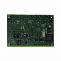
BOARD EVAL PM6670AS DDR2/3
Manufacturer
STMicroelectronics
Type
DC/DC Switching Converters, Regulators & Controllersr
Specifications of STEVAL-ISA051V2
Design Resources
STEVAL-ISA051V2 Gerber Files STEVAL-ISA051V2 Schematic STEVAL-ISA051V2 Bill of Material
Main Purpose
Special Purpose DC/DC, DDR Memory Supply
Outputs And Type
4, Non-Isolated
Voltage - Output
1.5V, 1.8V
Voltage - Input
4.5 ~ 36V
Regulator Topology
Buck
Board Type
Fully Populated
Utilized Ic / Part
PM6670A
Input Voltage
4.5 V to 36 V
Output Voltage
1.8 V, 1.5 V
Product
Power Management Modules
Silicon Manufacturer
ST Micro
Silicon Core Number
PM6670AS
Kit Application Type
Power Management
Application Sub Type
DDR2/3 Memory Power Supply Controller
Kit Contents
Board
Lead Free Status / RoHS Status
Lead free / RoHS Compliant
Current - Output
-
Power - Output
-
Frequency - Switching
-
Lead Free Status / Rohs Status
Lead free / RoHS Compliant
For Use With/related Products
PM6670AS
Other names
497-8412
Available stocks
Company
Part Number
Manufacturer
Quantity
Price
Company:

Part Number:
STEVAL-ISA051V2
Manufacturer:
STMicroelectronics
Quantity:
1


PM6670AS
7.1.2
Figure 28. Switching section simplified block diagram
Output ripple compensation and loop stability
The loop is closed connecting the center tap of the output divider (internally, when the fixed
output voltage is chosen, or externally, using the MODE pin in the adjustable output voltage
mode). The feedback node is the negative input of the error comparator, while the positive
input is internally connected to the reference voltage (Vr = 0.9 V). When the feedback
voltage becomes lower than the reference voltage, the PWM comparator goes to high and
sets the control logic, turning on the high-side MOSFET. After the On-Time (calculated as
previously described) the system releases the high-side MOSFET and turns on the
synchronous rectifier.
The voltage drop along ground and supply PCB paths, used to connect the output capacitor
to the load, is a source of DC error. Furthermore the system regulates the output voltage
valley, not the average, as shown in
capacitor is an additional source of DC error. To compensate this error, an integrative
network is introduced in the control loop, by connecting the output voltage to the COMP pin
through a capacitor (C
INT
) as shown in
Doc ID 14436 Rev 2
Figure 26
Figure 29
. Thus, the voltage ripple on the output
.
Device description
23/53
Related parts for STEVAL-ISA051V2
Image
Part Number
Description
Manufacturer
Datasheet
Request
R

Part Number:
Description:
BOARD RGB CTR ST7,STP08C596MTR
Manufacturer:
STMicroelectronics
Datasheet:

Part Number:
Description:
Power Management IC Development Tools Full Speed USB to RS232 Bridge Demo
Manufacturer:
STMicroelectronics
Datasheet:
Part Number:
Description:
Power Management IC Development Tools 2.5W solar eval BRD USB SPV1040 LD39050
Manufacturer:
STMicroelectronics
Datasheet:

Part Number:
Description:
BOARD EVAL FOR MEMS SENSORS
Manufacturer:
STMicroelectronics
Datasheet:

Part Number:
Description:
KIT DEV STARTER ST10F276Z5
Manufacturer:
STMicroelectronics
Datasheet:

Part Number:
Description:
BOARD EVAL HDMI $ VIDEO SWITCH
Manufacturer:
STMicroelectronics
Datasheet:

Part Number:
Description:
BOARD DEMO ACCELEROMETER DIL24
Manufacturer:
STMicroelectronics
Datasheet:

Part Number:
Description:
BOARD STLM75/STDS75/ST72F651
Manufacturer:
STMicroelectronics
Datasheet:

Part Number:
Description:
EVAL BOARD 3AXIS MEMS ACCELLRMTR
Manufacturer:
STMicroelectronics
Datasheet:

Part Number:
Description:
BOARD EVAL 8BIT MICRO + TDE1708
Manufacturer:
STMicroelectronics
Datasheet:
Part Number:
Description:
STMicroelectronics [RIPPLE-CARRY BINARY COUNTER/DIVIDERS]
Manufacturer:
STMicroelectronics
Datasheet:
Part Number:
Description:
STMicroelectronics [LIQUID-CRYSTAL DISPLAY DRIVERS]
Manufacturer:
STMicroelectronics
Datasheet:
Part Number:
Description:
BOARD EVAL FOR MEMS SENSORS
Manufacturer:
STMicroelectronics
Datasheet: