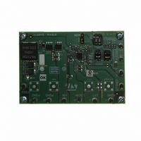
STEVAL-ISA051V1 STMicroelectronics, STEVAL-ISA051V1 Datasheet
STEVAL-ISA051V1
Specifications of STEVAL-ISA051V1
Available stocks


Related parts for STEVAL-ISA051V1


STEVAL-ISA051V1 Summary of contents
Page 1
Complete DDR2/3 memory power supply controller Features ■ Switching section (VDDQ) – 4 input voltage range – 0.9 V, ±1 % voltage reference – 1.8 V (DDR2) or 1.5 V (DDR3) fixed output voltages – 0.9 ...
Page 2
Contents Contents 1 Typical application circuit . . . . . . . . . . . . . . . . . . . . . . . . . . . . . . . . . . ...
Page 3
PM6670S 7.3 S3 and S5 power management pins . . . . . . . . . . . . . . . . . . . . . . . . . . . . 38 8 Application information ...
Page 4
Typical application circuit 1 Typical application circuit Figure 1. Application circuit VDDQ ( LDO input IN4 23 4 VTTREF 2 C OUT3 24 VTT 1 C OUT2 4/54 + IN3 IN2 ...
Page 5
PM6670S 2 Pin settings 2.1 Connections Figure 2. Pin connection (through top view VTTGND VTTGND VTTSNS VTTSNS DDRSEL DDRSEL PM6670 PM6670 VTTREF VTTREF SGND SGND AVCC AVCC Doc ID 14432 Rev 4 ...
Page 6
Pin settings 2.2 Pin description Table 2. Pin functions N° Pin 1 VTTGND 2 VTTSNS 3 DDRSEL 4 VTTREF 5 SGND 6 AVCC 7 VREF 8 VOSC 9 VSNS 10 MODE 11 COMP 12 DSCG ...
Page 7
PM6670S Table 2. Pin functions (continued) N° Pin 18 VCC 19 CSNS 20 PHASE 21 HGATE 22 BOOT 23 LDOIN 24 VTT +5 V low-side gate driver supply. Bypass with a 100 nF capacitor to PGND. Current sense input for ...
Page 8
Electrical data 3 Electrical data 3.1 Maximum rating Table 3. Absolute maximum ratings Symbol V AVCC V VCC V PHASE P TOT 1. Free air operating conditions unless otherwise specified. Stresses beyond those listed under “absolute maximum ratings” may cause ...
Page 9
PM6670S 3.3 Recommended operating conditions Table 5. Recommended operating conditions Symbol V Input voltage range supply voltage AVCC V IC supply voltage VCC Parameter Doc ID 14432 Rev 4 Electrical data Values Unit Min Typ Max 4.5 ...
Page 10
Electrical characteristics 4 Electrical characteristics ° °C, VCC = AVCC = +5 V and LDOIN connected to VDDQ output if not A otherwise specified Table 6. Electrical characteristics Symbol Parameter Supply section I Operating current ...
Page 11
PM6670S Table 6. Electrical characteristics (continued) Symbol Parameter VDDQ output VDDQ output voltage, DDR3 V VDDQ VDDQ output voltage, DDR2 Feedback accuracy Current limit and zero crossing comparator I CSNS input bias current CSNS Comparator offset Positive current limit threshold ...
Page 12
Electrical characteristics Table 6. Electrical characteristics (continued) Symbol Parameter Soft end section VDDQ discharge resistance in non-tracking discharge mode VTT discharge resistance in non-tracking discharge mode VTTREF discharge resistance in non-tracking discharge mode VDDQ output threshold synchronous for final tracking ...
Page 13
PM6670S Table 6. Electrical characteristics (continued) Symbol Parameter LDO source current limit I VTT,CL LDO sink current limit VTTREF section VTTREF output voltage V VTTREF output voltage VTTREF accuracy respect to VSNS/2 I VTTREF current limit VTTREF Power management section ...
Page 14
Typical operating characteristics 5 Typical operating characteristics Figure 3. Efficiency vs load - 1.5 V and 1 100 100 ...
Page 15
PM6670S Figure 9. VDDQ load regulation, 1 1.860 1.860 1.850 1.850 1.840 1.840 1.830 1.830 1.820 1.820 1.810 1.810 1.800 1.800 0.001 0.001 0.01 0.01 0.1 0.1 Output current (A) Output current (A) Figure ...
Page 16
Typical operating characteristics Figure 15. Power-up sequence - AVCC above UVLO Figure 17. -1 1.8 A VTT load transient, 0.9 V 16/54 Figure 16. VDDQ soft-start, 1.8 V, heavy load Figure 18 VTTREF ...
Page 17
PM6670S Figure 19. Non-tracking (soft) discharge Figure 21 VDDQ load transient, PWM Typical operating characteristics Figure 20. Tracking (fast) discharge, LDOIN = VDDQ Figure 22 VDDQ load transient, PWM Doc ...
Page 18
Typical operating characteristics Figure 23 VDDQ load transient, pulse-skip Figure 25. Over-voltage protection, VDDQ = 1.8 V 18/54 Figure 24 VDDQ load transient, pulse-skip Figure 26. Under-voltage protection, VDDQ = ...
Page 19
PM6670S 6 Block diagram Figure 27. Functional and block diagram VTTSNS VTTSNS LDOIN LDOIN VTT VTT VTTGND VTTGND VTTREF VTTREF SGND SGND AVCC AVCC DDRSEL DDRSEL DSCG DSCG Table 7. Legend SWEN Switching controller enable TD Tracking discharge enable NTD ...
Page 20
Device description 7 Device description The PM6670SS is designed to satisfy DDR2-3 power supply requirements combining a synchronous buck controller buffered reference and a high-current low-drop out (LDO) linear regulator capable of sourcing and sinking up to ...
Page 21
PM6670S 7.1 VDDQ section - constant on-time PWM controller The PM6670S uses a pseudo-fixed frequency, constant on-time (COT) controller as the core of the switching section well known that the COT controller uses a relatively simple algorithm and ...
Page 22
Device description The duty-cycle of the buck converter is, in steady-state conditions, given by Equation 2 The switching frequency is thus calculated as Equation 3 where Equation 4a Equation 4b Referring to the typical application schematic (figures on cover page ...
Page 23
PM6670S 7.1.1 Constant-on-time architecture Figure 30 shows the simplified block diagram of the constant-on-time controller. The switching regulator of the PM6670S owns a one-shot generator that ignites the high- side MOSFET when the following conditions are simultaneously satisfied: the PWM ...
Page 24
Device description 7.1.2 Output ripple compensation and loop stability The loop is closed connecting the center tap of the output divider (internally, when the fixed output voltage is chosen, or externally, using the MODE pin in the adjustable output voltage ...
Page 25
PM6670S The design of the external feedback network depends on the output voltage ripple. If the ripple is higher than approximately 20 mV, the correct CINT capacitor is usually enough to keep the loop stable. The stability of the system ...
Page 26
Device description Figure 32. “Virtual-ESR” network T NODE VOLTAGE ΔV 1 The ripple on the COMP pin is the sum of the output voltage ripple and the triangular ripple generated by the Virtual-ESR network. In fact the Virtual-ESR Network behaves ...
Page 27
PM6670S Equation 14 Moreover, the C INT Equation 15 where R is the sum of the ESR of the output capacitor and the equivalent ESR given by TOT the Virtual-ESR Network (R determines the minimum integrator capacitor value C Equation ...
Page 28
Device description 7.1.3 Pulse-skip and no-audible pulse-skip modes High efficiency at light load conditions is achieved by PM6670S entering the pulse-skip mode (if enabled). When one of the two fixed output voltages is set, pulse-skip power saving is a default ...
Page 29
PM6670S No-audible pulse-skip mode Some audio-noise sensitive applications cannot accept the switching frequency to enter the audible range as is possible in pulse-skip mode with very light loads. For this reason, the PM6670S implements an additional feature to maintain a ...
Page 30
Device description 7.1.4 Mode-of-operation selection Figure 35. MODE and DDRSEL multifunction pin configurations VDDQ VDDQ The PM6670S has been designed to satisfy the widest range of applications involving DDR2/3 memories, SSTL15-18 buses termination and I/O supplies ...
Page 31
PM6670S VDDQ output voltage can be set in the range of 0 2.6 V. Adjustable mode automatically switches DDRSEL pin to become the power saving algorithm selector: if tied the forced-PWM (fixed frequency) control is ...
Page 32
Device description Referring to Figure 36 without the need for an external sensing resistor. The on-resistance of the MOSFET is affected by temperature drift and nominal value spread of the parameter itself; this must be considered during the R It ...
Page 33
PM6670S After a fixed 3 ms total time, the soft-start finishes and UVP is released: if the output voltage doesn't reach the under voltage threshold within soft-start duration, the UVP condition is detected and the device performs a soft end ...
Page 34
Device description 7.1.8 VDDQ output discharge Active discharge of VDDQ output occurs when PM6670S enters the suspend-to-disk system state (S3 and S5 tied to GND) and DSCG pin has been properly set. Figure 39. DSCG pin connection for discharge mode ...
Page 35
PM6670S 7.1.9 Gate drivers The integrated high-current gate drivers allow using different power MOSFETs. The high- side driver uses a bootstrap circuit which is supplied by the +5 V rail. The BOOT and PHASE pins work respectively as supply and ...
Page 36
Device description 7.1.11 Over voltage and under voltage protections When the switching output voltage is about 115 % of its nominal value, a latched over- voltage protection (OVP) occurs. In this case the synchronous rectifier immediately turns on while the ...
Page 37
PM6670S 7.2 VTTREF buffered reference and VTT LDO section The PM6670S provides the required DDR2/3 reference voltage on the VTTREF pin. The internal buffer tracks half the voltage on the VSNS pin and has a sink and source capability up ...
Page 38
Device description 7.3 S3 and S5 power management pins According to DDR2/3 memories supply requirements, the PM6670S can manage all system states by connecting S3-S5 pins to their respective sleep-mode signals in the notebook motherboard. Keeping S3 ...
Page 39
PM6670S 8 Application information The purpose of this chapter is to show the design procedure of the switching section. The design starts from three main specifications: ● The input voltage range, provided by the battery or the AC adapter. The ...
Page 40
Application information where Equation 27a Equation 27b Referring to the typical application schematic (figure in cover page and expression is then: Equation 28 The switching frequency directly affects two parameters: ● Inductor size: greater frequencies mean smaller inductances. In notebook ...
Page 41
PM6670S 8.1.1 Inductor selection Once the switching frequency has been defined, the inductance value depends on the desired inductor ripple current. Low inductance value means great ripple current that brings poor efficiency and great output noise. On the other hand ...
Page 42
Application information The saturation current of the inductor should be greater than I saturation core inductors. Using soft-ferrite cores it is possible (but not advisable) to push the inductor working near its saturation current. In Table 13 some inductors suitable ...
Page 43
PM6670S It must be taken into account that in some MLCC the capacitance decreases when the operating voltage is near the rated voltage. In applications are listed. Table 14. Evaluated MLCC for input filtering Manufacturer TAIYO YUDEN UMK325BJ106KM-T TAIYO YUDEN ...
Page 44
Application information If ceramic capacitors are used, the output voltage ripple due to inductor current ripple is negligible. Then the inductance could be smaller, reducing the size of the choke. In this case it is important that output capacitor can ...
Page 45
PM6670S where R is the drain-source on-resistance of the control MOSFET. DSon Switching losses are approximately given by: Equation 41 P switching where t and t ON OFF gate-driver current capability and the gate charge Q low R . Unfortunately ...
Page 46
Application information Tested low-side MOSFETs are listed in Table 17. Evaluated low-side MOSFETs Manufacturer ST STS12NH3LL ST STS25NH3LL IR Dual N-MOS can be used in applications with lower output current. Table 18 shows some suitable dual MOSFETs for applications requiring ...
Page 47
PM6670S 8.1.6 VDDQ current limit setting The valley current limit is set by R current. The valley of the inductor current I Equation 45 The output current limit depends on the current ripple as shown in Figure 41. Valley current ...
Page 48
Application information 8.1.7 All ceramic capacitors application Design of external feedback network depends on the output voltage ripple across the output capacitors' ESR. If the ripple is great enough (at least 20 mV), the compensation network simply consists of a ...
Page 49
PM6670S If the ripple on pin COMP is greater than the integrator output dynamic (150 mV), an additional capacitor C attenuation factor of the output ripple, select: Equation 50 In order to reduce noise on pin COMP, it's possible to ...
Page 50
Application information Select C as shown: Equation 52 Then calculate R in order to have enough ripple voltage on the integrator input: Equation 53 Where R is the new virtual output capacitor ESR. A good trade-off is to consider an ...
Page 51
PM6670S 9 Package mechanical data In order to meet environmental requirements, ST offers these devices in different grades of ® ECOPACK packages, depending on their level of environmental compliance. ECOPACK specifications, grade definitions and product status are available at: www.st.com. ...
Page 52
Package mechanical data Figure 44. Package dimensions 52/54 Doc ID 14432 Rev 4 PM6670S ...
Page 53
PM6670S 10 Revision history Table 21. Document revision history Date 06-Feb-2008 23-Feb-2009 30-Oct-2009 03-Feb-2010 Revision 1 Initial release 2 Updated Table 3 on page 8 3 Updated package drawing in cover page, Updated Table 2 on page 4 21, Figure ...
Page 54
... Information in this document is provided solely in connection with ST products. STMicroelectronics NV and its subsidiaries (“ST”) reserve the right to make changes, corrections, modifications or improvements, to this document, and the products and services described herein at any time, without notice. All ST products are sold pursuant to ST’s terms and conditions of sale. ...