LM5118EVAL/NOPB National Semiconductor, LM5118EVAL/NOPB Datasheet - Page 14
LM5118EVAL/NOPB
Manufacturer Part Number
LM5118EVAL/NOPB
Description
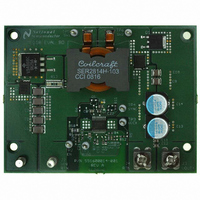
BOARD EVALUATION FOR LM5118
Manufacturer
National Semiconductor
Series
PowerWise®r
Specifications of LM5118EVAL/NOPB
Main Purpose
DC/DC, Step Up or Down
Outputs And Type
1, Non-Isolated
Voltage - Output
12V
Current - Output
3A
Voltage - Input
5 ~ 75V
Regulator Topology
Buck-Boost
Frequency - Switching
300kHz
Board Type
Fully Populated
Utilized Ic / Part
LM5118
Lead Free Status / RoHS Status
Not applicable / Not applicable
Power - Output
-
Other names
*LM5118EVAL
LM5118EVAL
LM5118EVAL


www.national.com
Error Amplifier and PWM
Comparator
The internal high gain error amplifier generates an error signal
proportional to the difference between the regulated output
voltage and an internal precision reference (1.23V). The out-
put of the error amplifier is connected to the COMP pin. Loop
compensation components, typically a type II network illus-
Ramp Generator
The ramp signal of a pulse-width modulator with current mode
control is typically derived directly from the buck switch drain
current. This switch current corresponds to the positive slope
portion of the inductor current signal. Using this signal for the
PWM ramp simplifies the control loop transfer function to a
single pole response and provides inherent input voltage
feed-forward compensation. The disadvantage of using the
buck switch current signal for PWM control is the large leading
edge spike due to circuit parasitics. The leading edge spike
must be filtered or blanked to avoid early termination of the
PWM pulse. Also, the current measurement may introduce
significant propagation delays. The filtering, blanking time
and propagation delay limit the minimal achievable pulse
width. In applications where the input voltage may be rela-
tively large in comparison to the output voltage, controlling a
small pulse width is necessary for regulation. The LM5118
utilizes a unique ramp generator which does not actually
measure the buck switch current but instead creates a signal
representing or emulating the inductor current. The emulated
ramp provides signal to the PWM comparator that is free of
leading edge spikes and measurement or filtering delays. The
current reconstruction is comprised of two elements, a sam-
ple-and-hold pedestal level and a ramp capacitor which is
charged by a controlled current source. Refer to
details.
The sample-and-hold pedestal level is derived from a mea-
surement of the re-circulating current through a current sense
resistor in series with the re-circulating diode of the buck reg-
ulator stage. A small value current sensing resistor is required
between the re-circulating diode anode and ground. The CS
FIGURE 9. Composition of Emulated Current Signal
Figure 9
for
14
trated in
pins. This network creates a low frequency pole, a zero, and
a noise reducing high frequency pole. The PWM comparator
compares the emulated current sense signal from the RAMP
generator to the error amplifier output voltage at the COMP
pin. The same error amplifier is used for operation in buck and
buck-boost mode.
and CSG pins should be Kelvin connected directly to the
sense resistor. The voltage level across the sense resistor is
sampled and held just prior to the onset of the next conduction
interval of the buck switch. The current sensing and sample-
and-hold provide the DC level of the reconstructed current
signal. The sample and hold of the re-circulating diode current
is valid for both buck and buck-boost modes. The positive
slope inductor current ramp is emulated by an external ca-
pacitor connected from the RAMP pin to the AGND and an
internal voltage controlled current source. In buck mode, the
ramp current source that emulates the inductor current is a
function of the VIN and VOUT voltages per the following
equation:
In buck-boost mode, the ramp current source is a function of
the input voltage VIN, per the following equation:
Proper selection of the RAMP capacitor (C
on the value of the output inductor (L) and the current sense
resistor (R
hold pedestal value and the ramp amplitude must have the
same relative relationship to the actual inductor current. That
is:
Figure 1
S
). For proper current emulation, the sample and
are connected between the COMP and FB
30058525
RAMP
) depends up-
Related parts for LM5118EVAL/NOPB
Image
Part Number
Description
Manufacturer
Datasheet
Request
R

Part Number:
Description:
National Semiconductor [8-Bit D/A Converter]
Manufacturer:
National Semiconductor
Datasheet:
Part Number:
Description:
National Semiconductor [Media Coprocessor]
Manufacturer:
National Semiconductor
Datasheet:
Part Number:
Description:
Digitally Controlled Tone and Volume Circuit with Stereo Audio Power Amplifier, Microphone Preamp Stage and National 3D Sound
Manufacturer:
National Semiconductor
Datasheet:
Part Number:
Description:
Digitally Controlled Tone and Volume Circuit with Stereo Audio Power Amplifier, Microphone Preamp Stage and National 3D Sound
Manufacturer:
National Semiconductor
Datasheet:
Part Number:
Description:
AC97 Rev 2 Codec with Sample Rate Conversion and National 3D Sound
Manufacturer:
National Semiconductor
Part Number:
Description:
Manufacturer:
National Semiconductor
Datasheet:
Part Number:
Description:
Manufacturer:
National Semiconductor
Datasheet:
Part Number:
Description:
General Purpose, Low Voltage, Low Power, Rail-to-Rail Output Operational Amplifiers
Manufacturer:
National Semiconductor
Datasheet:
Part Number:
Description:
8-bit 20 MSPS flash A/D converter.
Manufacturer:
National Semiconductor
Datasheet:
Part Number:
Description:
Low Noise Quad Operational Amplifier
Manufacturer:
National Semiconductor
Datasheet:
Part Number:
Description:
Quad Differential Line Receivers
Manufacturer:
National Semiconductor
Datasheet:
Part Number:
Description:
Quad High Speed Trapezoidal? Bus Transceiver
Manufacturer:
National Semiconductor
Datasheet:
Part Number:
Description:
Dual Line Receiver
Manufacturer:
National Semiconductor
Datasheet:
Part Number:
Description:
TTL to 10k ECL Level Translator with Latch
Manufacturer:
National Semiconductor
Datasheet: