LM5118EVAL/NOPB National Semiconductor, LM5118EVAL/NOPB Datasheet - Page 12
LM5118EVAL/NOPB
Manufacturer Part Number
LM5118EVAL/NOPB
Description
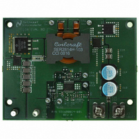
BOARD EVALUATION FOR LM5118
Manufacturer
National Semiconductor
Series
PowerWise®r
Specifications of LM5118EVAL/NOPB
Main Purpose
DC/DC, Step Up or Down
Outputs And Type
1, Non-Isolated
Voltage - Output
12V
Current - Output
3A
Voltage - Input
5 ~ 75V
Regulator Topology
Buck-Boost
Frequency - Switching
300kHz
Board Type
Fully Populated
Utilized Ic / Part
LM5118
Lead Free Status / RoHS Status
Not applicable / Not applicable
Power - Output
-
Other names
*LM5118EVAL
LM5118EVAL
LM5118EVAL


www.national.com
High Voltage Start-Up Regulator
The LM5118 contains a dual mode, high voltage linear regu-
lator that provides the VCC bias supply for the PWM controller
and the MOSFET gate driver. The VIN input pin can be con-
nected directly to input voltages as high as 75V. For input
voltages below 10V, an internal low dropout switch connects
VCC directly to VIN. In this supply range, VCC is approxi-
mately equal to VIN. For VIN voltages greater than 10V, the
low dropout switch is disabled and the VCC regulator is en-
abled to maintain VCC at approximately 7V. A wide operating
range of 4V to 75V (with a startup requirement of at least 5
volts) is achieved through the use of this dual mode regulator.
The output of the VCC regulator is current limited to 35 mA,
typical. Upon power up, the regulator sources current into the
capacitor connected to the VCC pin. When the voltage at the
VCC pin exceeds the VCC under-voltage threshold of 3.7V
and the UVLO input pin voltage is greater than 1.23V, the gate
driver outputs are enabled and a soft-start sequence begins.
The gate driver outputs remain enabled until VCC falls below
3.5V or the voltage at the UVLO pin falls below 1.13V.
In many applications the regulated output voltage or an aux-
iliary supply voltage can be applied to the VCCX pin to reduce
the IC power dissipation. For output voltages between 4V and
15V, VOUT can be connected directly to VCCX. When the
voltage at the VCCX pin is greater than 3.85V, the internal
VCC regulator is disabled and an internal switch connects
VCCX to VCC, reducing the internal power dissipation.
In high voltage applications extra care should be taken to en-
sure the VIN pin voltage does not exceed the absolute max-
FIGURE 5. Buck (HO) and Boost (LO) Switch Duty Cycle vs. Time,
Illustrating Gradual Mode Change with Decreasing Input Voltage
12
imum voltage rating of 76V. During line or load transients,
voltage ringing on the VIN line that exceeds the absolute
maximum rating can damage the IC. Both careful PC board
layout and the use of quality bypass capacitors located close
to the VIN and GND pins are essential.
Enable
The LM5118 contains an enable function which provides a
very low input current shutdown mode. If the EN pin is pulled
below 0.5V, the regulator enters shutdown mode, drawing
less than 10 µA from the VIN pin. Raising the EN input above
FIGURE 6. VIN and VCC Sequencing
30058555
30058516
Related parts for LM5118EVAL/NOPB
Image
Part Number
Description
Manufacturer
Datasheet
Request
R

Part Number:
Description:
National Semiconductor [8-Bit D/A Converter]
Manufacturer:
National Semiconductor
Datasheet:
Part Number:
Description:
National Semiconductor [Media Coprocessor]
Manufacturer:
National Semiconductor
Datasheet:
Part Number:
Description:
Digitally Controlled Tone and Volume Circuit with Stereo Audio Power Amplifier, Microphone Preamp Stage and National 3D Sound
Manufacturer:
National Semiconductor
Datasheet:
Part Number:
Description:
Digitally Controlled Tone and Volume Circuit with Stereo Audio Power Amplifier, Microphone Preamp Stage and National 3D Sound
Manufacturer:
National Semiconductor
Datasheet:
Part Number:
Description:
AC97 Rev 2 Codec with Sample Rate Conversion and National 3D Sound
Manufacturer:
National Semiconductor
Part Number:
Description:
Manufacturer:
National Semiconductor
Datasheet:
Part Number:
Description:
Manufacturer:
National Semiconductor
Datasheet:
Part Number:
Description:
General Purpose, Low Voltage, Low Power, Rail-to-Rail Output Operational Amplifiers
Manufacturer:
National Semiconductor
Datasheet:
Part Number:
Description:
8-bit 20 MSPS flash A/D converter.
Manufacturer:
National Semiconductor
Datasheet:
Part Number:
Description:
Low Noise Quad Operational Amplifier
Manufacturer:
National Semiconductor
Datasheet:
Part Number:
Description:
Quad Differential Line Receivers
Manufacturer:
National Semiconductor
Datasheet:
Part Number:
Description:
Quad High Speed Trapezoidal? Bus Transceiver
Manufacturer:
National Semiconductor
Datasheet:
Part Number:
Description:
Dual Line Receiver
Manufacturer:
National Semiconductor
Datasheet:
Part Number:
Description:
TTL to 10k ECL Level Translator with Latch
Manufacturer:
National Semiconductor
Datasheet: