STEVAL-IFW001V1 STMicroelectronics, STEVAL-IFW001V1 Datasheet - Page 38
STEVAL-IFW001V1
Manufacturer Part Number
STEVAL-IFW001V1
Description
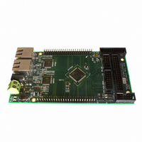
BOARD EVAL BASED ON STR912FA
Manufacturer
STMicroelectronics
Datasheets
1.STEVAL-IFW001V1.pdf
(102 pages)
2.STEVAL-IFW001V1.pdf
(9 pages)
3.STEVAL-IFW001V1.pdf
(7 pages)
Specifications of STEVAL-IFW001V1
Design Resources
STEVAL-IFW001V1 Gerber Files STEVAL-IFW001V1 Schematic STEVAL-IFW001V1 Bill of Material
Main Purpose
Interface, Ethernet
Embedded
Yes, MCU, 32-Bit
Utilized Ic / Part
E-STE101P, STR912FAW44
Primary Attributes
Dual Ethernet Transceivers for Full Duplex Communication
Secondary Attributes
Up to 32 MII Addresses, UART, I2C, SPI, with RJ45 Connectors
Silicon Manufacturer
ST Micro
Core Architecture
ARM
Core Sub-architecture
ARM9
Silicon Core Number
STR9
Silicon Family Name
STR91x
For Use With
497-8263 - BOARD EXTENSION STEVAL-IFW001V1
Lead Free Status / RoHS Status
Lead free / RoHS Compliant
Other names
497-8262


Functional overview
3.27
38/102
External memory interface (EMI)
STR91xFA devices in 128-pin and 144-ball packages offer an external memory bus for
connecting external parallel peripherals and memories. The EMI bus resides on ports 7, 8,
and 9 and operates with either an 8 or 16-bit data path. The configuration of 8 or 16 bit
mode is specified by CPU firmware writing to configuration registers at run-time. If the
application does not use the EMI bus, then these port pins may be used for general purpose
I/O as shown in
The EMI has the following features:
●
●
●
●
●
To use all 24 address bits, the following applies: 8 bits of lowest-order data and 8 bits of
lowest-order address are multiplexed on port 8. On port 9, 8-bits of mid-order address are
multiplexed with 8 bits of data, but these 8 data values are always at logic zero on this port
during a write operation, and these 8 data bits are ignored during a read operation. An
external latch device is needed to de-multiplex the mid-order 8 address bits that are
generated on port 8. Port 7 outputs the 8 highest-order address signals directly (not
multiplexed). The output signal on pin EMI_ALE is used to demultiplex the signals on ports 8
and 9, and the polarity of EMI_ALE is programmable. The output signal on pin
Supports static asynchronous memory access cycles, including page mode for non-
mux operation. The bus control signals include:
–
–
–
–
Four configurable memory regions, each with a chip select output (EMI_CS0n ...
EMI_CS3n)
Programmable wait states per memory region for both write and read operations
16-bit multiplexed data mode
address are multiplexed together on ports 8 and 9, while port 7 contains eight more
high-order address signals. The output signal on pin EMI_ALE is used to demultiplex
the signals on ports 8 and 9, and the polarity of EMI_ALE is programmable. The output
signals on pins EMI_BWR_WRLn and EMI_WRHn are the write strobes for the low and
high data bytes respectively. The output signal EMI_RDn is the read strobe for both the
low and high data bytes.
8-bit multiplexed data mode: This is a variant of the 16-bit multiplexed mode.
Although this mode can provide 24 bits of address and 8 bits of data, it does require an
external latch device on Port 8. However, this mode is most efficient when connecting
devices that only require 8 bits of address on an 8-bit multiplexed address/data bus,
and have simple read, write, and latch inputs as shown in
EMI_RDn - read signal, x8 or x16 mode
EMI_BWR_WRLn - write signal in x8 mode and write low byte signal in x16 mode
EMI_WRHn - write high byte signal in x16 mode
EMI_ALE - address latch signal for x8 or x16 mux bus mode with programmable
polarity
Table
8.
Doc ID 13495 Rev 6
(Figure
4): 16 bits of data and 16 bits of low-order
Figure 5
STR91xFAxxx
Related parts for STEVAL-IFW001V1
Image
Part Number
Description
Manufacturer
Datasheet
Request
R

Part Number:
Description:
BOARD EVAL SPZB260 MOD FOR STR9
Manufacturer:
STMicroelectronics
Datasheet:

Part Number:
Description:
BOARD EVAL EXTENSION SN250
Manufacturer:
STMicroelectronics
Datasheet:

Part Number:
Description:
BOARD EVAL AB-54003L-512
Manufacturer:
STMicroelectronics
Datasheet:

Part Number:
Description:
BOARD REF DESIGN RF DMOS PWR AMP
Manufacturer:
STMicroelectronics
Datasheet:

Part Number:
Description:
BOARD EVAL PWR AMP AB-84008L-470
Manufacturer:
STMicroelectronics
Datasheet:

Part Number:
Description:
BOARD EVAL FOR STM32F103XX
Manufacturer:
STMicroelectronics
Datasheet:

Part Number:
Description:
BOARD EVAL AB-54003L-512
Manufacturer:
STMicroelectronics
Datasheet:

Part Number:
Description:
BOARD SMART PLUG STM32 SPZB260PR
Manufacturer:
STMicroelectronics
Datasheet:

Part Number:
Description:
BOARD DEMO BLUETOOTH SPBT2532C2
Manufacturer:
STMicroelectronics
Datasheet:
Part Number:
Description:
ZIGBEE USB DONGLE EVAL KIT
Manufacturer:
STMicroelectronics
Datasheet:
Part Number:
Description:
STMicroelectronics [RIPPLE-CARRY BINARY COUNTER/DIVIDERS]
Manufacturer:
STMicroelectronics
Datasheet:
Part Number:
Description:
STMicroelectronics [LIQUID-CRYSTAL DISPLAY DRIVERS]
Manufacturer:
STMicroelectronics
Datasheet:

Part Number:
Description:
BOARD EVAL FOR MEMS SENSORS
Manufacturer:
STMicroelectronics
Datasheet: