CDB8421 Cirrus Logic Inc, CDB8421 Datasheet - Page 6
CDB8421
Manufacturer Part Number
CDB8421
Description
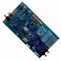
BOARD EVAL FOR CS8421
Manufacturer
Cirrus Logic Inc
Datasheet
1.CDB8421.pdf
(22 pages)
Specifications of CDB8421
Main Purpose
Audio, Sample Rate Converter
Embedded
No
Utilized Ic / Part
CS8421, CS8406, CS8416
Primary Attributes
Sample Rate Converter with Digital Audio Transmitter and Receiver
Secondary Attributes
S/PDIF Interface
Description/function
Audio DSPs
Operating Supply Voltage
3 V to 5 V
Product
Audio Modules
For Use With/related Products
CS8421
Lead Free Status / RoHS Status
Contains lead / RoHS non-compliant
Lead Free Status / RoHS Status
Lead free / RoHS Compliant, Contains lead / RoHS non-compliant
Other names
598-1018


6
8421_OUPUT_PCM
8421_INPUT_PCM
8421_MCLK_OUT
1.7
1.8
Switch S4 allows any of the PCM clocks/data to be turned off, selection between the OPTI-
CAL and COAXIAL S/PDIF inputs, bypassing the CS8421 sample rate converter, and turning
off the CS8421 MCLK_OUT signal. To input and output S/PDIF to and from the CS8421, the
switches labeled 8416_PCM, 8421_INPUT_PCM, 8421_OUTPUT_PCM, and 8406_PCM
should all be set in the CLOSED position. The functions for switches S4[6:0] are detailed in
Table 5.
NOTE:The reset button must be pressed before a new mode of operation takes affect.
Some speed modes and switch combinations are not compatible with the CS8416, CS8421,
or the CS8406. LED’s D4, D5, and D7 indicate that a switch setting is not compatible with the
corresponding part.
Power must be supplied to the evaluation board through the +5.0 V binding post (J1). On-
board regulators supply +3.3 V and +2.5 V to the rest of the board. Jumper J3 sets the VL
supply of the CS8416, CS8421, and CS8406 to either +3.3 V or +5.0 V. All voltage inputs
must be referenced to the single black banana-type ground connector (J2).
WARNING:Please refer to the CS8421 data sheet for allowable voltage levels.
The CS8421 requires careful attention to power supply and grounding arrangements to opti-
mize performance. Figure 1 provides an overview of the connections to the CS8421,
Figure 10 shows the component placement, Figure 11 shows the top layout, and Figure 12
shows the bottom layout. The decoupling capacitors are located as close to the CS8421 as
possible. Extensive use of ground plane fill in the evaluation board yields large reductions in
radiated noise.
8421_BYPASS
Switch Name
8416_RXSEL
8416_PCM
8406_PCM
Power
Grounding and Power Supply Decoupling
Selects Coaxial Connector (J5) for S/PDIF
Selects CS8421 SRC Bypass Mode (no
Inhibits Clock I/O and Data Output from
Inhibits Clock I/O and Data Output from
Inhibits Clock I/O and Data Output from
Inhibits Clock I/O and Data Input from
CS8421 MCLK_OUT Pin Held Low
sample rate conversion)
CS8421 to Header J11
Header J11 to CS8406
CS8416 to Header J8
Header J8 to CS8421
Table 5. Switch S4, Board Setup
OPEN
Input
Selects Optical Receiver (J12) for S/PDIF
Allows Clock I/O and Data Output from
Allows Clock I/O and Data Output from
Allows Clock I/O and Data Output from
Allows Clock I/O and Data Input from
Selects CS8421 SRC Active Mode
CS8421 MCLK_OUT Pin Active
CS8421 to Header J11
Header J11 to CS8406
CS8416 to Header J8
Header J8 to CS8421
CLOSED
Input
CDB8421
DS641DB3
Related parts for CDB8421
Image
Part Number
Description
Manufacturer
Datasheet
Request
R

Part Number:
Description:
Development Kit
Manufacturer:
Cirrus Logic Inc
Datasheet:
Part Number:
Description:
Development Kit
Manufacturer:
Cirrus Logic Inc
Datasheet:


Part Number:
Description:
High-efficiency PFC + Fluorescent Lamp Driver Reference Design
Manufacturer:
Cirrus Logic Inc
Datasheet:
Part Number:
Description:
Development Kit
Manufacturer:
Cirrus Logic Inc
Datasheet:
Part Number:
Description:
Development Kit
Manufacturer:
Cirrus Logic Inc
Datasheet:

Part Number:
Description:
Development Kit
Manufacturer:
Cirrus Logic Inc
Datasheet:
Part Number:
Description:
Development Kit
Manufacturer:
Cirrus Logic Inc
Datasheet:
Part Number:
Description:
Development Kit
Manufacturer:
Cirrus Logic Inc
Datasheet:
Part Number:
Description:
Development Kit
Manufacturer:
Cirrus Logic Inc
Datasheet:

Part Number:
Description:
EVALUATION BOARD FOR CS8427
Manufacturer:
Cirrus Logic Inc
Datasheet:

Part Number:
Description:
BOARD EVAL FOR CS8416 RCVR
Manufacturer:
Cirrus Logic Inc
Datasheet:

Part Number:
Description:
EVALUATION BOARD FOR CS8420
Manufacturer:
Cirrus Logic Inc
Datasheet:

Part Number:
Description:
KIT DEVELOPMENT EP9315 ARM9
Manufacturer:
Cirrus Logic Inc
Datasheet:

Part Number:
Description:
KIT DEVELOPMENT EP9302 ARM9
Manufacturer:
Cirrus Logic Inc
Datasheet: