CDB8421 Cirrus Logic Inc, CDB8421 Datasheet - Page 4
CDB8421
Manufacturer Part Number
CDB8421
Description
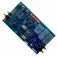
BOARD EVAL FOR CS8421
Manufacturer
Cirrus Logic Inc
Datasheet
1.CDB8421.pdf
(22 pages)
Specifications of CDB8421
Main Purpose
Audio, Sample Rate Converter
Embedded
No
Utilized Ic / Part
CS8421, CS8406, CS8416
Primary Attributes
Sample Rate Converter with Digital Audio Transmitter and Receiver
Secondary Attributes
S/PDIF Interface
Description/function
Audio DSPs
Operating Supply Voltage
3 V to 5 V
Product
Audio Modules
For Use With/related Products
CS8421
Lead Free Status / RoHS Status
Contains lead / RoHS non-compliant
Lead Free Status / RoHS Status
Lead free / RoHS Compliant, Contains lead / RoHS non-compliant
Other names
598-1018


4
CS8421 Input Port CS8421 Output Port CS8421 XTI/XTO Clock Source
1.4
1.5
1.6
Table 1 shows the available I/O configurations and their respective clock sources. When the
CS8416 is selected to master SCLK and LRCK (CS8421 input port set to slave), J7 should
be set to 8416. When the CS8421 input port is selected to master SCLK and LRCK (CS8416
set to slave), J7 may be set to 8416, OSC, or XTAL. When the CS8406 is selected to master
SCLK and LRCK (CS8421 output port set to slave), J13 should be set to OSC. When the
CS8421 output port is selected to master SCLK and LRCK (CS8406 set to slave), J13 should
be set to 8421. The board is shipped with a 24.576 MHz crystal/oscillator stuffed at Y1, Y2,
and Y3.
The CDB8421 includes headers for input (J8) and output (J11) port clocks and data. These
headers can enabled/disabled using S4. When not using these headers, SDIN should be
jumpered to SDOUT on both J8 and J11. The pin functions for headers J8 and J11 are shown
in Table 7.
The CDB8421 also includes a header for TDM operation (J16). Refer to the CS8421 data
sheet for possible TDM configurations [1]. This header can enabled/disabled using J14.
All headers operate at the VL supply, therefore any external circuit connected to these head-
ers should also operate at VL.
The CPLD (U2) controls all of the configuration for the CS8421, CS8416, and CS8406. The
CPLD decodes switches S1, S2, S3, and S4 and sets the appropriate mode of operation.
Switch S1 controls the master/slave and MCLK/LRCK ratio settings for the CS8421, CS8416,
and CS8406. The functions for S1[3:0] are detailed in Table 2.
Master
Slave
Slave
S1[3:0]
0000
0001
0010
0011
0100
1000
1001
1010
1011
Clocking
Clock and Data Headers
CPLD Board Setup
Table 2. Switch S1, Serial Input and Output Master/Slave and Speed Mode Settings
Master
Slave
Slave
Master (Master Clock = 128*Fs)
Master (Master Clock = 256*Fs)
Master (Master Clock = 384*Fs)
Master (Master Clock = 512*Fs)
CS8421 Input
Slave
Slave
Slave
Slave
Slave
Table 1. Clock Sources
CS8416 RMCK, Y1, or Y2
CS8416 RMCK, Y1, or Y2
CS8416 RMCK
Master (Master Clock = 128*Fs)
Master (Master Clock = 256*Fs)
Master (Master Clock = 384*Fs)
Master (Master Clock = 512*Fs)
Y3
CS8421 MCLK_OUT
Y3
CS8406 OMCK Clock Source
CS8421 Output
Slave
Slave
Slave
Slave
Slave
CDB8421
DS641DB3
Related parts for CDB8421
Image
Part Number
Description
Manufacturer
Datasheet
Request
R

Part Number:
Description:
Development Kit
Manufacturer:
Cirrus Logic Inc
Datasheet:
Part Number:
Description:
Development Kit
Manufacturer:
Cirrus Logic Inc
Datasheet:


Part Number:
Description:
High-efficiency PFC + Fluorescent Lamp Driver Reference Design
Manufacturer:
Cirrus Logic Inc
Datasheet:
Part Number:
Description:
Development Kit
Manufacturer:
Cirrus Logic Inc
Datasheet:
Part Number:
Description:
Development Kit
Manufacturer:
Cirrus Logic Inc
Datasheet:

Part Number:
Description:
Development Kit
Manufacturer:
Cirrus Logic Inc
Datasheet:
Part Number:
Description:
Development Kit
Manufacturer:
Cirrus Logic Inc
Datasheet:
Part Number:
Description:
Development Kit
Manufacturer:
Cirrus Logic Inc
Datasheet:
Part Number:
Description:
Development Kit
Manufacturer:
Cirrus Logic Inc
Datasheet:

Part Number:
Description:
EVALUATION BOARD FOR CS8427
Manufacturer:
Cirrus Logic Inc
Datasheet:

Part Number:
Description:
BOARD EVAL FOR CS8416 RCVR
Manufacturer:
Cirrus Logic Inc
Datasheet:

Part Number:
Description:
EVALUATION BOARD FOR CS8420
Manufacturer:
Cirrus Logic Inc
Datasheet:

Part Number:
Description:
KIT DEVELOPMENT EP9315 ARM9
Manufacturer:
Cirrus Logic Inc
Datasheet:

Part Number:
Description:
KIT DEVELOPMENT EP9302 ARM9
Manufacturer:
Cirrus Logic Inc
Datasheet: