EVAL-ADCMP581BCPZ Analog Devices Inc, EVAL-ADCMP581BCPZ Datasheet - Page 4
EVAL-ADCMP581BCPZ
Manufacturer Part Number
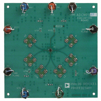
EVAL-ADCMP581BCPZ
Description
BOARD EVALUATION ADCMP581BCP
Manufacturer
Analog Devices Inc
Specifications of EVAL-ADCMP581BCPZ
Main Purpose
Interface, Comparator
Utilized Ic / Part
ADCMP581
Lead Free Status / RoHS Status
Lead free / RoHS Compliant
Secondary Attributes
-
Embedded
-
Primary Attributes
-


ADCMP580/ADCMP581/ADCMP582
Parameter
AC PERFORMANCE
POWER SUPPLY
1
Equivalent input bandwidth assumes a simple first-order input response and is calculated with the following formula: BW
transition time of a quasi-Gaussian input edge applied to the comparator input and tr
ADCMP582 (PECL)
Propagation Delay
Propagation Delay Temperature Coefficient
Propagation Delay Skew—Rising
Overdrive Dispersion
Slew Rate Dispersion
Pulse Width Dispersion
Duty Cycle Dispersion 5% to 95%
Common-Mode Dispersion
Equivalent Input Bandwidth
Toggle Rate
Deterministic Jitter
Deterministic Jitter
RMS Random Jitter
Minimum Pulse Width
Minimum Pulse Width
Rise/Fall Time
Positive Supply Voltage
Negative Supply Voltage
ADCMP580 (CML)
ADCMP581 (NECL)
ADCMP582 (PECL)
Logic Supply Voltage
Positive Supply Current
Negative Supply Current
Power Dissipation
Positive Supply Current
Negative Supply Current
Power Dissipation
Input Supply Current
Output Supply Current
Negative Supply Current
Power Dissipation
Power Supply Rejection (V
Power Supply Rejection (V
Power Supply Rejection (V
Output Voltage High Level
Output Voltage High Level
Output Voltage High Level
Output Voltage Low Level
Output Voltage Low Level
Output Voltage Low Level
Output Voltage Differential
Transition to Falling Transition
1
CCI
EE
CCO
)
)
)
Symbol
V
V
V
V
V
V
t
Δt
BW
DJ
DJ
RJ
PW
PW
t
V
V
I
I
P
I
I
P
V
I
I
I
P
PSR
PSR
PSR
VCCI
VEE
VCCI
VEE
VCCI
VCCO
VEE
PD
R,
OH
OH
OH
OL
OL
OL
CCI
EE
D
D
CCO
D
PD
t
F
EQ
MIN
MIN
VCCI
VEE
VCCO
/d
T
Condition
V
50 Ω to V
50 Ω to V
50 Ω to V
50 Ω to V
50 Ω to V
50 Ω to V
50 Ω to V
V
V
50 mV < V
10 mV < V
2 V/ns to 10 V/ns
100 ps to 5 ns
1.0 V/ns, 15 MHz, V
V
0.0 V to 400 mV input,
t
>50% output swing
V
PRBS
V
PRBS
V
Δt
Δt
20/80
V
V
50 Ω to GND
V
V
50 Ω to −2 V
V
V
V
50 Ω to V
V
V
V
Rev. A | Page 4 of 16
R
OD
CCO
OD
OD
OD
OD
OD
CCI
EE
CCI
EE
CCI
CCO
EE
CCI
EE
CCO
= t
PD
PD
= −5.0 V, 50 Ω to GND
= −5.0 V, 50 Ω to −2 V
= −5.0 V, 50 Ω to V
= −5.0 V + 5%
= 200 mV, 5 V/ns, 1.25 GHz
= 500 mV
= 500 mV, 5 V/ns
= 0.2 V, −2 V < V
= 500 mV, 5 V/ns,
= 200 mV, 5 V/ns,
= 5.0 V, 50 Ω to GND
= 5.0 V, 50 Ω to −2 V
= 5.0 V, 50 Ω to V
= 5.0 V + 5%
= 3.3 V
< 5 ps
< 10 ps
= 5.0 V, 50 Ω to V
= 3.3 V + 5% (ADCMP582)
F
31
31
= 25 ps, 20/80
− 1 NRZ, 5 Gbps
− 1 NRZ, 10 Gbps
COMP
CCO
CCO
CCO
CCO
CCO
CCO
CCO
CCO
OD
OD
− 2 V, T
− 2 V, T
− 2 V, T
is the effective transition time digitized by the comparator.
− 2 V, T
− 2 V, T
− 2 V, T
− 2.0 V
− 2 V
< 1.0 V
< 200 mV
CM
A
A
A
A
A
A
CM
= 125°C
= 25°C
= −55°C
= 125°C
= 25°C
= −55°C
CCO
= 0.0 V
CCO
CCO
< 3 V
− 2 V
− 2 V
− 2 V
Min
V
V
V
V
V
V
340
+4.5
−5.5
−50
−35
+2.5
−35
CCO
CCO
CCO
CCO
CCO
CCO
EQ
− 0.99
− 1.06
− 1.11
− 1.43
− 1.50
− 1.55
= 0.22/(tr
Typ
V
V
V
V
V
V
395
180
0.25
10
10
15
15
15
10
5
8
12.5
15
25
0.2
100
80
37
+5.0
−5.0
6
−40
230
6
−25
155
+3.3
6
44
−25
310
−75
−60
−75
COMP
CCO
CCO
CCO
CCO
CCO
CCO
2
– tr
− 0.87
− 0.94
− 0.99
− 1.26
− 1.33
− 1.35
IN
2
), where tr
Max
V
V
V
V
V
V
450
+5.5
−4.5
8
−34
260
8
−19
200
+5.0
8
55
−19
350
CCO
CCO
CCO
CCO
CCO
CCO
IN
− 0.75
− 0.82
− 0.87
− 1.13
− 1.20
− 1.25
is the 20/80
Unit
V
V
V
V
V
V
mV
ps
ps/°C
ps
ps
ps
ps
ps
ps
ps/V
GHz
Gbps
ps
ps
ps
ps
ps
ps
V
V
mA
mA
mW
mA
mA
mW
V
mA
mA
mA
mW
dB
dB
dB
Related parts for EVAL-ADCMP581BCPZ
Image
Part Number
Description
Manufacturer
Datasheet
Request
R

Part Number:
Description:
IC, ADJ LDO REG, 1.5V TO 5V 250mA MSOP-8
Manufacturer:
Vishay
Datasheet:

Part Number:
Description:
IC, ADJ LDO REG, 1.5V TO 5V 0.6A 8-TSSOP
Manufacturer:
Vishay
Datasheet:
Part Number:
Description:
IC, ADJ LDO REG, 1.5V TO 5V 250mA MSOP-8
Manufacturer:
Vishay
Datasheet:

Part Number:
Description:
IC ADJ LDO REG 1.5V TO 5V 150mA 5-SOT-23
Manufacturer:
Vishay
Datasheet:

Part Number:
Description:
BOARD EVAL AS1324-AD
Manufacturer:
austriamicrosystems
Datasheet:
Part Number:
Description:
IC, ADJ LDO REG, 1.5V TO 5V 0.6A 8-TSSOP
Manufacturer:
Vishay
Datasheet:

Part Number:
Description:
IC, ADJ LDO REG, 1.5V TO 5V, 0.3A, MSOP8
Manufacturer:
Vishay
Datasheet:
Part Number:
Description:
IC, ADJ LDO REG, 1.5V TO 5V, 0.3A, MSOP8
Manufacturer:
Vishay
Datasheet:
Part Number:
Description:
IC, ADJ LDO REG 1.215V TO 5V 0.3A MSOP-8
Manufacturer:
Vishay
Datasheet:
Part Number:
Description:
IC, ADJ LDO REG 1.215V TO 5V 0.3A MSOP-8
Manufacturer:
Vishay
Datasheet:

Part Number:
Description:
±1.7g Dual-Axis IMEMS Accelerometer Evaluation Board
Manufacturer:
Analog Devices Inc
Datasheet:

Part Number:
Description:
IC MULTIPLIER ANALOG 8-SOIC T/R
Manufacturer:
Analog Devices Inc
Datasheet:

Part Number:
Description:
IC ANALOG MULTIPLIER 8-DIP
Manufacturer:
Analog Devices Inc
Datasheet:
Part Number:
Description:
IC ANALOG MULTIPLIER 8-SOIC
Manufacturer:
Analog Devices Inc
Datasheet:
Part Number:
Description:
IC ANALOG MULTIPLIER 8-DIP
Manufacturer:
Analog Devices Inc
Datasheet: