CDB5467U Cirrus Logic Inc, CDB5467U Datasheet - Page 6
CDB5467U
Manufacturer Part Number
CDB5467U
Description
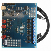
BOARD EVAL FOR CS5467 ADC
Manufacturer
Cirrus Logic Inc
Type
A/Dr
Specifications of CDB5467U
Main Purpose
Power Management, Energy/Power Meter
Embedded
Yes, MCU, 8-Bit
Utilized Ic / Part
CS5467
Primary Attributes
Watt-Hour Meter
Secondary Attributes
Graphical User Interface, SPI™ & USB Interfaces
Product
Data Conversion Development Tools
Maximum Clock Frequency
4 MHz
Interface Type
USB
Supply Voltage (max)
5 V
Supply Voltage (min)
3.3 V
For Use With/related Products
CS5467
Lead Free Status / RoHS Status
Contains lead / RoHS non-compliant
Lead Free Status / RoHS Status
Lead free / RoHS Compliant, Contains lead / RoHS non-compliant
Other names
598-1555
CDB-5467U
CDB-5467U


2. PIN DESCRIPTION
6
Clock Generator
Crystal Out
Crystal In
CPU Clock Output
Control Pins and Serial Data I/O
Serial Clock
Serial Data Output
Chip Select
Mode Select
Energy Output
Reset
Interrupt
Serial Data Input
Analog Inputs/Outputs
Differential Voltage Inputs
Differential Current Inputs
Voltage Reference Output
Voltage Reference Input
Power Supply Connections
Positive Digital Supply
Digital Ground
Positive Analog Supply
Analog Ground
Power Fail Monitor
Voltage Reference Output
Differential Voltage Input
Differential Voltage Input
Differential Voltage Input
Differential Voltage Input
Voltage Reference Input
Positive Digital Supply
CPU Clock Output
Serial Data Ouput
Digital Ground
Mode Select
Serial Clock
Chip Select
Crystal Out
22, 25,
13, 14
20,19,
16,15
1,28
9,10
26
23
24
27
11
12
18
17
21
2
5
6
7
8
3
4
XOUT, XIN — Connect to an external quartz crystal. Alternatively, an external clock can be sup-
plied to the XIN pin to provide the system clock for the device.
CPUCLK — Logic-level output from crystal oscillator. Can be used to clock an external CPU.
SCLK — Clocks serial data from the SDI pin and to the SDO pin when CS is low. SCLK is a
Schmitt-trigger input when MODE is low and a driven output when MODE is high.
SDO — Serial data output. Data is clocked out by SCLK.
CS — An input that enables the serial interface when MODE is low and a driven output when
MODE is high.
MODE — High selects external E
weak internal pull-down and therefore selects microcontroller mode if not connected.
E3, E1, E2 — Primarily active-low energy pulse outputs. These can be programmed to output
other conditions.
RESET — An active-low Schmitt-trigger input used to reset the chip.
INT — Active-low output, indicates that an enabled condition has occurred.
SDI — Serial data input. Data is clocked in by SCLK.
VIN1+, VIN1-, VIN2+, VIN2- — Differential analog inputs for the voltage channels.
IIN1+, IIN1-, IIN2+, IIN2- — Differential analog inputs for the current channels.
VREFOUT — The on-chip voltage reference output. Nominally 2.5 V, referenced to AGND.
VREFIN — The voltage reference input. Can be connected to VREFOUT or external 2.5 V refer-
ence.
VD+ — The positive digital supply.
DGND — Digital ground.
VA+ — The positive analog supply.
AGND — Analog ground.
PFMON — Used to monitor the unregulated power supply via a resistive divider. If the PFMON
voltage drops below its low limit, the low-supply detect (LSD) bit is set in the Status register.
VREFOUT
CPUCLK
VREFIN
MODE
DGND
XOUT
VIN1+
VIN2+
SCLK
VIN2-
VIN1-
SDO
VD+
CS
13
14
1
2
3
4
5
6
7
8
9
10
11
12
28
27
26
25
24
23
22
21
20
19
18
17
16
15
2
PROM, Low selects external microcontroller. MODE includes a
IIN2+
IIN2-
XIN
SDI
E2
E1
INT
RESET
E3
PFMON
IIN1+
IIN1-
VA+
AGND
Crystal In
Serial Data Input
Energy Output 2
Energy Output 1
Interrupt
Reset
Energy Output 3
Power Fail Monitor
Differential Current Input
Differential Current Input
Positive Analog Supply
Analog Ground
Differential Current Input
Differential Current Input
CS5467
DS714F1
Related parts for CDB5467U
Image
Part Number
Description
Manufacturer
Datasheet
Request
R

Part Number:
Description:
Development Kit
Manufacturer:
Cirrus Logic Inc
Datasheet:
Part Number:
Description:
Development Kit
Manufacturer:
Cirrus Logic Inc
Datasheet:


Part Number:
Description:
High-efficiency PFC + Fluorescent Lamp Driver Reference Design
Manufacturer:
Cirrus Logic Inc
Datasheet:
Part Number:
Description:
Development Kit
Manufacturer:
Cirrus Logic Inc
Datasheet:
Part Number:
Description:
Development Kit
Manufacturer:
Cirrus Logic Inc
Datasheet:

Part Number:
Description:
Development Kit
Manufacturer:
Cirrus Logic Inc
Datasheet:
Part Number:
Description:
Development Kit
Manufacturer:
Cirrus Logic Inc
Datasheet:
Part Number:
Description:
Development Kit
Manufacturer:
Cirrus Logic Inc
Datasheet:
Part Number:
Description:
Development Kit
Manufacturer:
Cirrus Logic Inc
Datasheet:

Part Number:
Description:
EVALUATION BOARD FOR CS8427
Manufacturer:
Cirrus Logic Inc
Datasheet:

Part Number:
Description:
BOARD EVAL FOR CS8416 RCVR
Manufacturer:
Cirrus Logic Inc
Datasheet:

Part Number:
Description:
EVALUATION BOARD FOR CS8420
Manufacturer:
Cirrus Logic Inc
Datasheet:

Part Number:
Description:
KIT DEVELOPMENT EP9315 ARM9
Manufacturer:
Cirrus Logic Inc
Datasheet:

Part Number:
Description:
KIT DEVELOPMENT EP9302 ARM9
Manufacturer:
Cirrus Logic Inc
Datasheet: