PBMCUSLK Freescale Semiconductor, PBMCUSLK Datasheet - Page 11
PBMCUSLK
Manufacturer Part Number
PBMCUSLK
Description
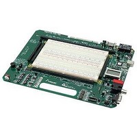
PROJECT BOARD FOR MCU
Manufacturer
Freescale Semiconductor
Datasheet
1.PBMCUSLK.pdf
(30 pages)
Specifications of PBMCUSLK
Module/board Type
Student Learning Kit
Silicon Manufacturer
Freescale
Core Architecture
HCS08, S12
Core Sub-architecture
HCS08, S12
Silicon Core Number
MC9S08, MC9S12
Silicon Family Name
S08QG, S12D
Rohs Compliant
Yes
For Use With/related Products
HC(S)12(X), HC(S)08, DSP, and ColdFire modules
Lead Free Status / RoHS Status
Lead free / RoHS Compliant


maximum current output of 1A while regulator VR2 is rated for a maximum current output of
500mA. In this configuration, ±15V is provided by the regulator at PS1. Both PS1 and VR2
derive their input from VR1.
applications. Each regulator is internally current limited to prevent damage from inadvertent,
short circuits of short duration. The regulator at PS1 is not protected from continuous short-
circuits on its output.
When connected to NI-ELVIS, the 5V rail is provided by the workstation. This input also drives
the 3.3V regulator at VR2. ±15V is available from the workstation and PS1 is not connected.
A 3-pin option header, VDD_SEL(JP3) shown in figure 2 allows the user to select the operating
voltage routed to VDD. The 5V selection routes 5VDC to on-board logic while the 3.3V
selection routes 3.3VDC to on-board logic.
around the prototype area to allowing easy access. ±15V voltage inputs are diode OR’ed and
available at connector J4.
Figure 2: VDD _SEL Option Header
±15V Power
The PBMCUSLK includes a DC-DC converter at PS1 to supply ±15V for use in analog circuit
construction and analysis. PS1 provides a maximum of 50mA on each output. PS1 draws its
input from the +5V rail. The option header 15V_EN
output if not needed. Disabling PS1 when not used conserves power and will prolong the life
of the +5V LDO at VR1.
Table 2: 15V_EN Option Header
*
Freescale Semiconductor
For project boards labeled MCU Project Board -2 AXM-0368 Rev C this jumper is labeled PS1_EN.
CAUTION: Exercise care to select the correct operating voltage when interfacing to on-board logic to prevent
Shunt
ON
OFF
JP3
Effect
Enables PS1 output to the project board
Disables PS1 output to the project board
1
2
●
+5V
+3.3V
Sets VDD to +5v
This setup may limit available current in mixed voltage
damaging circuit elements.
All voltage levels are conveniently arranged
JP3
●
2
3
+5V
+3.3V
*
(JP11) shown in table 2 disables the
Sets VDD to +3.3V
11
Related parts for PBMCUSLK
Image
Part Number
Description
Manufacturer
Datasheet
Request
R

Part Number:
Description:
Manufacturer:
Freescale Semiconductor, Inc
Datasheet:
Part Number:
Description:
Manufacturer:
Freescale Semiconductor, Inc
Datasheet:
Part Number:
Description:
Manufacturer:
Freescale Semiconductor, Inc
Datasheet:
Part Number:
Description:
Manufacturer:
Freescale Semiconductor, Inc
Datasheet:
Part Number:
Description:
Manufacturer:
Freescale Semiconductor, Inc
Datasheet:
Part Number:
Description:
Manufacturer:
Freescale Semiconductor, Inc
Datasheet:
Part Number:
Description:
Manufacturer:
Freescale Semiconductor, Inc
Datasheet:
Part Number:
Description:
Manufacturer:
Freescale Semiconductor, Inc
Datasheet:
Part Number:
Description:
Manufacturer:
Freescale Semiconductor, Inc
Datasheet:
Part Number:
Description:
Manufacturer:
Freescale Semiconductor, Inc
Datasheet:
Part Number:
Description:
Manufacturer:
Freescale Semiconductor, Inc
Datasheet:
Part Number:
Description:
Manufacturer:
Freescale Semiconductor, Inc
Datasheet:
Part Number:
Description:
Manufacturer:
Freescale Semiconductor, Inc
Datasheet:
Part Number:
Description:
Manufacturer:
Freescale Semiconductor, Inc
Datasheet:
Part Number:
Description:
Manufacturer:
Freescale Semiconductor, Inc
Datasheet: