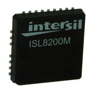
ISL8200MIRZ Intersil, ISL8200MIRZ Datasheet - Page 4

ISL8200MIRZ
Manufacturer Part Number
ISL8200MIRZ
Description
IC BUCK SYNC ADJ 10A 23-QFN
Manufacturer
Intersil
Type
Point of Load (POL) Non-Isolatedr
Datasheet
1.ISL8200MIRZ.pdf
(23 pages)
Specifications of ISL8200MIRZ
Output
0.6 ~ 6V
Number Of Outputs
1
Power (watts)
60W
Mounting Type
Surface Mount
Voltage - Input
3 ~ 20V
Package / Case
23-QFN
1st Output
0.6 ~ 6 VDC @ 10A
Size / Dimension
0.59" L x 0.59" W x 0.09" H (15mm x 15mm x 2.2mm)
Power (watts) - Rated
60W
Operating Temperature
-40°C ~ 85°C
Current - Output
10A
Voltage - Output
0.6 ~ 6 V
Frequency - Switching
700kHz ~ 1.5MHz
Synchronous Rectifier
Yes
Rohs Compliant
Yes
Lead Free Status / RoHS Status
Lead free / RoHS Compliant
3rd Output
-
2nd Output
-
Available stocks
Company
Part Number
Manufacturer
Quantity
Price
Part Number:
ISL8200MIRZ
Manufacturer:
INTERSIL
Quantity:
20 000
Pin Descriptions
NUMBER
PIN
10
11
12
13
14
16
17
18
19
20
6
7
8
9
ISHARE_BUS Open pin until first PWM pulse is generated. Then, via an internal FET, this pin connects the module’s
PIN NAME
PH_CNTRL
FSYNC IN
CLKOUT
ISHARE
PHASE
OCSET
PGND
VOUT
PVCC
PVIN
VIN
EN
FF
Analog Current Output - Cascaded system level over current shutdown pin. This pin is used where you
have multiple modules configured for current sharing and is used with a common current share bus.
The bus sums each of the modules' average current contribution to the load to protect for a over current
condition at the load. The pin sources 15µA plus average module's output current. The shared bus
voltage (VISHARE) is developed across an external resistor (RISHARE). VISHARE represents the
average current of all active channel(s) that connected together.
The ISHARE bus voltage is compared with each module's internal reference voltage set by each
module's RISET resistor. This will generate and individual current share error signal in each cascaded
controller. The share bus impedance RISHARE should be set as RISET/NCTRL, RISET divided by number
of active current sharing controllers. The output current from this pin generates a voltage across the
external resistor. This voltage, VISHARE, is compared to and internal 1.2V threshold for average
overcurrent protection. For full-scale current, RISHARE should be ~10kΩ . Typically 10kΩ is used for
RSHARE and RSET. Output Current Range: 15µA to 108µA typ.
Analog input Control Pin - An optional external resistor (RFS-ext) connected to this pin and ground will
increase the oscillator switching frequency. It has an internal 59kΩ resistor for a default frequency of
700kHz. The internal oscillator will lock to an external frequency source when connected to a square
wave form. The external source is typically the CLKOUT signal from another ISL8200M or an external
clock. The internal oscillator synchronizes with the leading positive edge of the input signal. Input
Voltage Range for external source: 0V to 5V Square Wave.
Digital Voltage Output - This pin provides a clock signal to synchronize with other ISL8200M(s). When
there is more than one ISL8200M in the system, the two independent regulators can be programmed
via PH_CNTRL for different degrees of phase delay.
Analog Input - The voltage level on this pin is used to program the phase shift of CLKOUT clock signal
to synchronize with other module(s).
ISHARE to the system’s ISHARE bus after pre-bias is complete and soft-start is initiated.
Analog Voltage Input - The voltages on this pin is fed into the controller, adjusting the sawtooth
amplitude to generate the feed-forward function. Voltage input 0.7 to V
This is a double function pin: Analog Input Voltage - The input voltage to this pin is compared with a
precision 0.8V reference and enables the digital soft-start. Input Voltage Range is 0V to V
through a pull up resistor maintaining a typical current of 5mA.
Analog Voltage Output - This pin can be used as a voltage monitor for input bus undervoltage lockout.
The hysteresis levels of the lockout can be programmed via this pin using a resistor divider network.
Furthermore, during fault conditions (such as overvoltage, overcurrent, and over-temperature), this
pin is used to communicate the information to other cascaded modules by pulling low the wired OR as
it is an Open Drain. Output Voltage Range is 0V to V
Analog Voltage Input - This pin should be tied directly to the input rail when using the internal linear
regulator. It provides power to the internal linear drive circuitry. When used with an external 5V supply,
this pin should be tied directly to VCC. The internal linear device is protected against the reversed bias
generated by the remained charge of the decoupling capacitor at VCC when losing the input rail. Input
Voltage Range 0V to 20V.
Analog Output - This pin is the output of the internal series linear regulator. It provides the bias for
both low-side and high-side drives. Its operational voltage range is 3V to 5.6V. The decoupling ceramic
capacitor in the PVCC pin is 10µF.
Analog Output = This pin is the phase node of the regulator. Output Voltage Range 0V to 30V.
Analog Input - This input voltage is applied to the power FETS with the FET’s ground being the PGND
pin. It is recommended to place input decoupling capacitance, 22µF, directly between PVIN pin and
PGND pin as close as possible to the module. Input Voltage Range: 0V to 20V.
All voltage levels are referenced to this pad. This is the low side MOSFET ground. PGND and PGND1
should be connected together with a ground plane.
Output voltage from the module. Output Voltage Range: 0.6V to 6V.
Analog Input - This pin is used with PHASE pin to set the current limit of the module. Input Voltage
Range 0V to 30V.
4
(Continued)
ISL8200M
PIN DESCRIPTION
CC
.
CC
.
February 26, 2010
CC
or V
FN6727.1
IN


