LMZ10503TZX-ADJ/NOPB National Semiconductor, LMZ10503TZX-ADJ/NOPB Datasheet - Page 12
LMZ10503TZX-ADJ/NOPB
Manufacturer Part Number
LMZ10503TZX-ADJ/NOPB
Description
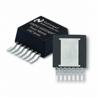
IC BUCK SYNC ADJ 3A TO-PMOD-7
Manufacturer
National Semiconductor
Series
SIMPLE SWITCHER®r
Type
Point of Load (POL) Non-Isolated with UVLOr
Datasheet
1.LMZ10503TZX-ADJNOPB.pdf
(22 pages)
Specifications of LMZ10503TZX-ADJ/NOPB
Output
0.8 ~ 5 V
Number Of Outputs
1
Power (watts)
15W
Mounting Type
Surface Mount
Voltage - Input
2.95 ~ 5.5 V
Package / Case
TO-PMOD-7, Power Module
1st Output
0.8 ~ 5 VDC @ 3A
Size / Dimension
0.40" L x 0.54" W x 0.18" H (10.16mm x 13.77mm x 4.57mm)
Power (watts) - Rated
15W
Operating Temperature
-40°C ~ 125°C
Efficiency
96%
Approvals
EN
Lead Free Status / RoHS Status
Lead free / RoHS Compliant
3rd Output
-
2nd Output
-
Other names
LMZ10503TZX-ADJ


www.national.com
Estimate Power Dissipation And
Board Thermal Requirements
Use the current derating curves in the typical performance
characteristics section to obtain an estimate of power loss
(P
I
must see a thermal resistance from case to ambient (θ
less than:
Given the typical thermal resistance from junction to case
(θ
greater than 125°C will have a shorten life span.
To reach θ
heat effectively. With no airflow and no external heat, a good
estimate of the required board area covered by 1oz. copper
on both the top and bottom metal layers is:
As a result, approximately 7.2 square cm of 1oz. copper on
top and bottom layers is required for the PCB design.
The PCB copper heat sink must be connected to the exposed
pad (EP). Approximately thirty six, 10mils (254 μm) thermal
vias spaced 59mils (1.5 mm) apart must connect the top cop-
per to the bottom copper. For an extended discussion and
formulations of thermal rules of thumb, refer to AN-2020. For
an example of a high thermal performance PCB layout with
θ
AN-2022 and for results of a study of the effects of the PCB
designs, refer to AN-2026.
PC Board Layout Guidelines
PC board layout is an important part of DC-DC converter de-
sign. Poor board layout can disrupt the performance of a DC-
DC converter and surrounding circuitry by contributing to EMI,
ground bounce and resistive voltage drop in the traces. These
can send erroneous signals to the DC-DC converter resulting
in poor regulation or instability. Good layout can be imple-
mented by following a few simple design rules.
OUT
JA
JC
IC_LOSS
of 20°C/W, refer to the evaluation board application note
) to be 1.9°C/W (typ.). Continuously operating at a T
= 3A, T
). For the design case of V
CA
A(MAX)
= 69.5°C/W, the PCB is required to dissipate
= 85°C , and T
J(MAX)
IN
= 5V, V
= 125°C, the device
OUT
= 2.5V,
CA
) of
J
12
1. Minimize area of switched current loops.
From an EMI reduction standpoint, it is imperative to minimize
the high di/dt current paths. The high current that does not
overlap contains high di/dt, see
place input capacitor (C
LMZ10503 VIN pin and GND exposed pad to avoid observ-
able high frequency noise on the output pin. This will minimize
the high di/dt area and reduce radiated EMI. Additionally,
grounding for both the input and output capacitor should con-
sist of a localized top side plane that connects to the GND
exposed pad (EP).
2. Have a single point ground.
The ground connections for the feedback, soft-start, and en-
able components should be routed only to the GND pin of the
device. This prevents any switched or load currents from
flowing in the analog ground traces. If not properly placed,
poor grounding can result in degraded load regulation or er-
ratic output voltage ripple behavior. Provide the single point
ground connection from pin 4 to EP.
3. Minimize trace length to the FB pin.
Both feedback resistors, R
components, R
FB pin. Since the FB node is high impedance, keep the copper
area as small as possible. This is most important as relatively
high value resistors are used to set the output voltage.
4. Make input and output bus connections as wide as
possible.
This reduces any voltage drops on the input or output of the
converter and maximizes efficiency. To optimize voltage ac-
curacy at the load, ensure that a separate feedback voltage
sense trace is made at the load. Doing so will correct for volt-
age drops and provide optimum output accuracy.
5. Provide adequate device heat-sinking.
Use an array of heat-sinking vias to connect the exposed pad
to the ground plane on the bottom PCB layer. If the PCB has
multiple copper layers, thermal vias can also be employed to
make connection to inner layer heat-spreading ground
planes. For best results use a 6 x 6 via array with minimum
via diameter of 10mils (254 μm) thermal vias spaced 59mils
(1.5 mm). Ensure enough copper area is used for heat-sinking
to keep the junction temperature below 125°C.
FIGURE 1. High Current Loops
comp
and C
comp
in1
fbt
) as close as possible to the
and R
, should be located close to the
Figure
fbb
, and the compensation
1. Therefore physically
301118b5
Related parts for LMZ10503TZX-ADJ/NOPB
Image
Part Number
Description
Manufacturer
Datasheet
Request
R

Part Number:
Description:
National Semiconductor [8-Bit D/A Converter]
Manufacturer:
National Semiconductor
Datasheet:
Part Number:
Description:
National Semiconductor [Media Coprocessor]
Manufacturer:
National Semiconductor
Datasheet:
Part Number:
Description:
Digitally Controlled Tone and Volume Circuit with Stereo Audio Power Amplifier, Microphone Preamp Stage and National 3D Sound
Manufacturer:
National Semiconductor
Datasheet:
Part Number:
Description:
Digitally Controlled Tone and Volume Circuit with Stereo Audio Power Amplifier, Microphone Preamp Stage and National 3D Sound
Manufacturer:
National Semiconductor
Datasheet:
Part Number:
Description:
AC97 Rev 2 Codec with Sample Rate Conversion and National 3D Sound
Manufacturer:
National Semiconductor
Part Number:
Description:
Manufacturer:
National Semiconductor
Datasheet:
Part Number:
Description:
Manufacturer:
National Semiconductor
Datasheet:
Part Number:
Description:
General Purpose, Low Voltage, Low Power, Rail-to-Rail Output Operational Amplifiers
Manufacturer:
National Semiconductor
Datasheet:
Part Number:
Description:
8-bit 20 MSPS flash A/D converter.
Manufacturer:
National Semiconductor
Datasheet:
Part Number:
Description:
Low Noise Quad Operational Amplifier
Manufacturer:
National Semiconductor
Datasheet:
Part Number:
Description:
Quad Differential Line Receivers
Manufacturer:
National Semiconductor
Datasheet:
Part Number:
Description:
Quad High Speed Trapezoidal? Bus Transceiver
Manufacturer:
National Semiconductor
Datasheet:
Part Number:
Description:
Dual Line Receiver
Manufacturer:
National Semiconductor
Datasheet:
Part Number:
Description:
TTL to 10k ECL Level Translator with Latch
Manufacturer:
National Semiconductor
Datasheet: