BP5222A Rohm Semiconductor, BP5222A Datasheet - Page 6
BP5222A
Manufacturer Part Number
BP5222A
Description
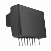
IC DC/DC CONV 12V 0.5A SIP9
Manufacturer
Rohm Semiconductor
Series
BP5222r
Type
Point of Load (POL) Non-Isolatedr
Datasheet
1.BP5222A.pdf
(9 pages)
Specifications of BP5222A
Output
12V
Number Of Outputs
1
Power (watts)
6W
Mounting Type
Through Hole
Voltage - Input
15 ~ 38V
Package / Case
9-SIP Module (8 Leads)
1st Output
12 VDC @ 500mA
Size / Dimension
1.10" L x 0.47" W x 0.77" H (28mm x 12mm x 19.5mm)
Power (watts) - Rated
6W
Operating Temperature
-20°C ~ 70°C
Efficiency
90%
Output Voltage
12 V
Output Current
0.5 A
Input Voltage
15 V to 38 V
Switching Frequency
190 KHz
Operating Temperature Range
- 20 C to + 70 C
Mounting Style
Through Hole
Lead Free Status / RoHS Status
Lead free / RoHS Compliant
3rd Output
-
2nd Output
-
Lead Free Status / Rohs Status
Lead free / RoHS Compliant


BP5220A/BP5221A/BP5222A
www.rohm.com
© 2010 ROHM Co., Ltd. All rights reserved.
(1) No circuit is installed in the modules to protect against excessive output currents. Therefore, take physical
(2) The output current should be reduced according to an increase in the input voltage or ambient temperature.
(3) A large rush current may flow in the module when the input voltage is applied or the output ON / OFF is
(4) Pins 5 and 7 are not connected.
(5) A smoothing electrolytic capacitor is necessary for I/O external components. Please use a capacitor equivalent
(6) Please put an I/O smoothing capacitor near the module. Output ripple voltage may be larger or output voltage
BP5220A
BP5221A
Operation notes
Electrical Characteristics Curves
safety measures such as using a fuse if short-circuit loading is probable.
Use the modules within the derating curve range.
controlled with pin 4 without a capacitor such as C1 in application 4. Operating within the safe operation
ranges shown in Fig.12, 15, and 18.
The safe operation range is determined by the safe operation range of the internal switching transistor.
The amount of rush current depends on the output impedance of the input power supply and capacitors
connected to the module outputs. The pulse load on the internal switching transistor at the start of operation
can be reduced by using the protection circuit in application 1 or the slow start circuit in application 4.
to the recommended one.
may not be stable.
1200
1000
800
600
400
200
0.6
0.5
0.4
0.3
0.2
0.1
0
0
Vi=34V
Vi=38V
AMBIENT TEMPERATURE : Ta( °C)
AMBIENT TEMPERATURE : Ta( °C)
25
25
Fig.10 Derating curve
Fig.13 Derating curve
50
50
Vi=8 to 15V
Vi=25V
Vi=30V
70
70
Vi=8 to 15V
Vi=30 to 38V
100
100
120
120
100
100
80
60
40
20
80
60
40
20
0
0
200
0.1
OUTPUT CURRENT : I
OUTPUT CURRENT : I
6/7
Fig.11 Efficiency
Fig.14 Efficiency
Vi=8V
Vi=23V
Vi=38V
400
0.2
Vi=8V
Vi=23V
Vi=38V
600
0.3
O
O
800
(A)
(A)
0.4
1000
0.5
4.5A
2.2A
0.5
0.3
0.2
0.1
0.1
20
10
10
5
3
2
1
1
1
1
Tc=25 °C
SINGLE PULSE
Tc=25 °C
SINGLE PULSE
VOLTAGE BETWEEN PIN2 AND PIN9 (V)
VOLTAGE BETWEEN PIN2 AND PIN9 (V)
Pw=1ms
Fig.12 Safety operation range
Fig.15 Safety operation range
Pw=10ms
2
3
5
10
10
Pw=1ms
2010.03 - Rev. B
Pw=0.2ms
20 30
Data Sheet
50
100
Related parts for BP5222A
Image
Part Number
Description
Manufacturer
Datasheet
Request
R

Part Number:
Description:
Manufacturer:
Rohm Semiconductor
Datasheet:
Part Number:
Description:
Manufacturer:
Rohm Semiconductor
Datasheet:
Part Number:
Description:
Manufacturer:
Rohm Semiconductor
Datasheet:
Part Number:
Description:
Manufacturer:
Rohm Semiconductor
Datasheet:
Part Number:
Description:
Manufacturer:
Rohm Semiconductor
Datasheet:
Part Number:
Description:
Manufacturer:
Rohm Semiconductor
Datasheet:
Part Number:
Description:
Manufacturer:
Rohm Semiconductor
Datasheet:
Part Number:
Description:
Manufacturer:
Rohm Semiconductor
Datasheet:
Part Number:
Description:
Manufacturer:
Rohm Semiconductor
Datasheet:
Part Number:
Description:
Manufacturer:
Rohm Semiconductor
Datasheet:
Part Number:
Description:
Manufacturer:
Rohm Semiconductor
Datasheet:
Part Number:
Description:
Manufacturer:
Rohm Semiconductor
Datasheet:

Part Number:
Description:
DIODE SWITCH 80V 25MA SMD5 TR
Manufacturer:
Rohm Semiconductor
Datasheet: