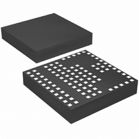
LTM4600HVIV#PBF Linear Technology, LTM4600HVIV#PBF Datasheet - Page 14

LTM4600HVIV#PBF
Manufacturer Part Number
LTM4600HVIV#PBF
Description
IC DC/DC UMODULE 10A 104-LGA
Manufacturer
Linear Technology
Series
µModuler
Type
Point of Load (POL) Non-Isolatedr
Datasheet
1.LTM4600HVEVPBF.pdf
(24 pages)
Specifications of LTM4600HVIV#PBF
Design Resources
LTM4600HV Spice Model
Output
0.6 ~ 5 V
Number Of Outputs
1
Power (watts)
50W
Mounting Type
Surface Mount
Voltage - Input
4.5 ~ 28 V
Package / Case
104-LGA
1st Output
0.6 ~ 5 VDC @ 10A
Size / Dimension
0.59" L x 0.59" W x 0.11" H (15mm x 15mm x 2.8mm)
Power (watts) - Rated
50W
Operating Temperature
-40°C ~ 85°C
Efficiency
92%
Lead Free Status / RoHS Status
Lead free / RoHS Compliant
3rd Output
-
2nd Output
-
Available stocks
Company
Part Number
Manufacturer
Quantity
Price
APPLICATIO S I FOR ATIO
LTM4600HV
In the application where the light load effi ciency is im-
portant, tying the FCB pin above 0.6V threshold enables
discontinuous operation where the bottom MOSFET turns
off when inductor current reverses. Therefore, the conduc-
tion loss is minimized and light load effi ciency is improved.
The penalty is that the controller may skip cycle and the
output voltage ripple increases at light load.
Paralleling Operation with Load Sharing
Two or more LTM4600HV modules can be paralleled to
provide higher than 10A output current. Figure 7 shows
the necessary interconnection between two paralleled
modules. The OPTI-LOOP™ current mode control en-
sures good current sharing among modules to balance
the thermal stress. The new feedback equation for two or
more LTM4600HVs in parallel is:
where N is the number of LTM4600HVs in parallel.
Thermal Considerations and Output Current Derating
The power loss curves in Figures 8 and 15 can be used
in coordination with the load current derating curves in
Figures 9 to 14, and Figures 16 to 19 for calculating an
approximate θ
ing methods. Thermal models are derived from several
temperature measurements at the bench, and thermal
modeling analysis. Application Note 103 provides a detailed
OPTI-LOOP is a trademark of Linear Technology Corporation.
14
V
OUT
V
Figure 7. Parallel Two μModules with Load Sharing
IN
=
0 6
.
V
JA
•
V
PGND
V
PGND
100
for the module with various heatsink-
IN
IN
U
N
R
k
COMP V
COMP V
LTM4600HV
LTM4600HV
SET
+
R
U
SET
OSET
OSET
R
SET
SGND
SGND
V
V
OUT
OUT
4600hv
W
F07
V
(20A
OUT
U
MAX
)
explanation of the analysis for the thermal models, and the
derating curves. Tables 3 and 4 provide a summary of the
equivalent θ
θ
improved with air-fl ow. The case temperature is maintained
at 100°C or below for the derating curves. This allows for
4W maximum power dissipation in the total module with
top and bottom heatsinking, and 2W power dissipation
through the top of the module with an approximate θ
between 6°C/W to 9°C/W. This equates to a total of 124°C
at the junction of the device.
Safety Considerations
The LTM4600HV modules do not provide isolation from
V
blow fuse with a rating twice the maximum input current
should be provided to protect each unit from catastrophic
failure.
Layout Checklist/Example
The high integration of the LTM4600HV makes the PCB
board layout very simple and easy. However, to optimize
its electrical and thermal performance, some layout con-
siderations are still necessary.
• Use large PCB copper areas for high current path, in-
• Place high frequency ceramic input and output capaci-
• Place a dedicated power ground layer underneath
• To minimize the via conduction loss and reduce module
• Do not put vias directly on pad unless they are capped.
• Use a separated SGND ground copper area for com-
Figure 20 gives a good example of the recommended
layout.
JA
IN
cluding V
PCB conduction loss and thermal stress
tors next to the V
high frequency noise
the unit
thermal stress, use multiple vias for interconnection
between top layer and other power layers
ponents connected to signal pins. Connect the SGND
to PGND underneath the unit
parameters are correlated to the measure values, and
to V
OUT
. There is no internal fuse. If required, a slow
JA
IN
, PGND and V
for the noted conditions. These equivalent
IN
, PGND and V
OUT
. It helps to minimize the
OUT
pins to minimize
4600hvfc
JC


