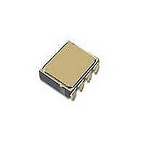
HCPL-5121-100 Avago Technologies US Inc., HCPL-5121-100 Datasheet - Page 12

HCPL-5121-100
Manufacturer Part Number
HCPL-5121-100
Description
ISOLAT 1.5KVDC 1CH TOTEM 8SMD BJ
Manufacturer
Avago Technologies US Inc.
Datasheet
1.HCPL-5120.pdf
(16 pages)
Specifications of HCPL-5121-100
Output Type
Push-Pull, Totem-Pole
Package / Case
8-SMD Butt Joint
Voltage - Isolation
1500VDC
Number Of Channels
1, Unidirectional
Current - Output / Channel
2A
Propagation Delay High - Low @ If
300ns @ 10mA ~ 18mA
Current - Dc Forward (if)
25mA
Input Type
DC
Mounting Type
Surface Mount
Configuration
1 Channel
Maximum Propagation Delay Time
500 ns
Maximum Forward Diode Voltage
1.8 V
Minimum Forward Diode Voltage
1.2 V
Maximum Reverse Diode Voltage
5 V
Maximum Forward Diode Current
18 mA
Maximum Power Dissipation
295 mW
Maximum Operating Temperature
+ 125 C
Minimum Operating Temperature
- 55 C
Number Of Elements
1
Forward Voltage
1.8V
Forward Current
25mA
Package Type
PDIP
Operating Temp Range
-55C to 125C
Power Dissipation
295mW
Propagation Delay Time
500ns
Pin Count
8
Mounting
Surface Mount
Reverse Breakdown Voltage
5V
Operating Temperature Classification
Military
Lead Free Status / RoHS Status
Contains lead / RoHS non-compliant
Lead Free Status / RoHS Status
Lead free / RoHS Compliant, Contains lead / RoHS non-compliant
Applications Information
Eliminating Negative IGBT Gate Drive
To keep the IGBT firmly off, the HCPL-520 has a very
low maximum V
realizes this very low V
with
When the HCPL-520 is in the low state, the IGBT gate
is shorted to the emitter by R
the lead inductance from the HCPL-520 to the IGBT
gate and emitter (possibly by mounting the HCPL-520
on a small PC board directly above the IGBT) can elimi-
nate the need for negative IGBT gate drive in many ap-
plications as shown in Figure 25. Care should be taken
with such a PC board design to avoid routing the IGBT
collector or emitter traces close to the HCPL-520 input
as this can result in unwanted coupling of transient sig-
nals into the HCPL-520 and degrade performance. (If
the IGBT drain must be routed near the HCPL-520 in-
put, then the LED should be reverse-biased when in the
off state, to prevent the transient signals coupled from
the IGBT drain from turning on the HCPL-520.)
Selecting the Gate Resistor (R
Switching Losses.
Step 1: Calculate R
ification.
The IGBT and R
RC circuit with a voltage supplied by the HCPL-520.
Figure 25. Recommended LED Drive and Application Circuit
2
CONTROL
INPUT
COLLECTOR
+5 V
R
74XXX
g
OPEN
Ω
= –––––––––––––––––
= ––––––––––––––––––
= –––––––––––––––––––
=
(typical) on resistance in its pull down circuit.
7.2Ω
(V
270 Ω
(V
CC
(15 V + 5 V – 2V)
I
CC
OLPEAK
g
- V
≈
in Figure 26 can be analyzed as a simple
– V
OL
EE
I
8Ω
OLPEAK
specification of 0.5 V. The HCPL-520
- V
2.5 A
EE
g
Minimum from the I
– 2V)
OL
1
2
3
4
)
OL
by using a DMOS transistor
g
+ Ω. Minimizing Rg and
g
) to Minimize IGBT
OL
Peak Spec-
8
7
6
5
0.1 µF
+
_
V
CC
Rg
= 18 V
The V
servative value of V
Figure 6). At lower Rg values the voltage supplied by
the HCPL-520 is not an ideal voltage step. This results
in lower peak currents (more margin) than predicted by
this analysis. When negative gate drive is not used V
the previous equation is equal to zero volts
Step 2: Check the HCPL-5120 Power Dissipation and
Increase R
The HCPL-520 total power dissipation (P
the sum of the emitter power (P
(P
P
P
P
For the circuit in Figure 26 with I
R
and T
P
P
The value of 4.25 mA for I
obtained by derating the I
at -55°C) to I
Since P
propriate.
T
E
O
g
E
O
O
= 18 mA • 1.8 V • 0.8 = 26 mW
< 112 mW (P
= P
= I
= P
= I
= 8 Ω, Max Duty Cycle = 80%, Q
= 4.25 mA • 20 V +
= 85 mW + 20 mW
= 105 mW
):
Q1
Q2
F
CC
A
E
•V
O(BIAS)
OL
+ P
max = 25°C:
• (V
O
F
value of 2 V in the previous equation is a con-
• Duty Cycle
for this case is less than P
O
+ P
g
CC
if Necessary.
CC
- V
O (SWITCHING)
O(MAX)
max at 25°C.
EE
) + ESW(R
@ 125°C = 250 mW - 23°C • 6 mW/°C)
OL
1.0µJ
at the peak current of 2.5A (see
CC
3-PHASE
g
+ HVDC
- HVDC
• 20 kHz
CC
, Q
in the previous equation was
AC
max of 5 mA (which occurs
g
) • f
E
) and the output power
F
(worst case) = 8 mA,
O(MAX)
g
= 500 nC, f = 20 kHz
, R
g
T
of 8
) is equal to
Ω
is ap-
EE
in


