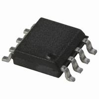
HCPL-0466#500 Avago Technologies US Inc., HCPL-0466#500 Datasheet - Page 13

HCPL-0466#500
Manufacturer Part Number
HCPL-0466#500
Description
OPTOCOUPLER IPM/DRVR 8-SOIC
Manufacturer
Avago Technologies US Inc.
Datasheet
1.HCPL-4506300.pdf
(21 pages)
Specifications of HCPL-0466#500
Output Type
Open Collector
Package / Case
8-SOIC (0.154", 3.90mm Width)
Voltage - Isolation
3750Vrms
Number Of Channels
1, Unidirectional
Current - Output / Channel
15mA
Data Rate
1MBd
Propagation Delay High - Low @ If
200ns @ 10mA
Current - Dc Forward (if)
25mA
Input Type
DC
Mounting Type
Surface Mount
Configuration
1 Channel
Isolation Voltage
3750 Vrms
Current Transfer Ratio
90 %
Maximum Propagation Delay Time
650 ns
Maximum Forward Diode Voltage
1.8 V
Maximum Reverse Diode Voltage
5 V
Maximum Forward Diode Current
20 mA
Maximum Continuous Output Current
15 mA
Maximum Power Dissipation
145 mW
Maximum Operating Temperature
+ 100 C
Minimum Operating Temperature
- 40 C
Lead Free Status / RoHS Status
Contains lead / RoHS non-compliant
Available stocks
Company
Part Number
Manufacturer
Quantity
Price
Switching Specifications (R
Over recommended operating conditions unless otherwise specified:
T
Switching Specifications (R
Over recommended operating conditions unless otherwise specified:
T
*All typical values at 25°C, V
†V
13
A
A
Parameter
Propagation Delay
Time to Logic
Low at Output
Propagation Delay
Time to High
Output Level
Pulse Width
Distortion
Propagation Delay
Difference Between
Any 2 Parts
Output High Level
Common Mode
Transient Immunity
Output Low Level
Common Mode
Transient Immunity
Parameter
Propagation Delay
Time to Logic
Low at Output
Propagation Delay Time
to High Output Level
Pulse Width
Distortion
Propagation Delay
Difference Between
Any 2 Parts
Output High Level
Common Mode
Transient Immunity
Output Low Level
Common Mode
Transient Immunity
Power Supply
Rejection
F(off )
= -40°C to +100°C, V
= -40°C to +100°C, V
= -3 V to 0.8 V for HCPL-J456, HCNW4506.
HCPL-J456
HCPL-J456
CC
L
CC
L
CC
= 20 kΩ External)
= Internal Pull-up)
= 15 V.
= +4.5 V to 30 V, I
= +4.5 V to 30 V, I
t
t
Symbol
Symbol
PLH
PLH
|CM
|CM
|CM
|CM
PWD
PWD
T
T
t
t
PSR
PHL
PLH
PHL
PLH
-t
-t
H
PHL
H
PHL
L
L
|
|
|
|
-150
-150
Min.
Min. Typ.*
270
220
30
15
15
20
F(on)
F(on)
= 10 mA to 20 mA, V
= 10 mA to 20 mA, V
Typ.*
200
100
400
130
200
200
200
450
250
250
1.0
30
30
30
30
Max. Units
400
485
650
500
500
Max. Units
400
480
550
450
450
kV/µs I
kV/µs I
kV/µs
kV/µs
V
ns
ns
ns
ns
p-p
ns
ns
ns
ns
F(off )
F(off )
I
V
V
V
V
Square Wave, t
> 5 ns, no bypass capacitors
F(on)
F
F
CC
O
O
THLH
C
C
C
C
C
I
V
I
V
= 0 mA,
= 16 mA,
F
F
L
L
L
L
L
O
O
> 3.0 V
< 1.0 V
= 0 mA,
= 10 mA
= 15.0 V, C
= 100 pF
= 10 pF
= 100 pF
= 10 pF
= 100 pF
= -5 V to 0.8 V†
> 3.0 V
< 1.0 V
= -5 V to 0.8 V†
= 10 mA, V
= 2.0 V, V
Test Conditions
Test Conditions
L
RISE
THHL
= 100 pF,
F(off )
V
C
V
T
A
CC
L
CM
, t
I
V
V
V
V
V
C
V
T
= 25°C
= 100 pF,
F(on)
A
= 1.5 V
FALL
F(off )
CC
THLH
THHL
CC
L
CM
= 15.0 V,
= 0.8 V,
= 1500 V
= 25°C
= 100 pF,
= 15.0 V,
= 15.0 V,
= 1500 V
= 10 mA,
= 0.8 V,
= 2.0 V,
= 1.5 V
p-p
p-p
,
6, 8,
6, 9
Fig.
Fig.
10-
13
7
7
11-14,
Note
Note
11,
14,
16
20
17
18
19
16
20
17
18
19
16


