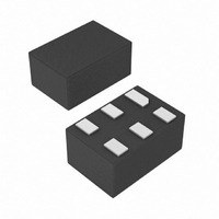
MAX4926ELT+T Maxim Integrated Products, MAX4926ELT+T Datasheet - Page 4

MAX4926ELT+T
Manufacturer Part Number
MAX4926ELT+T
Description
IC CTLR OVP W/EXT PFET 6-UDFN
Manufacturer
Maxim Integrated Products
Datasheet
1.MAX4925ELTT.pdf
(7 pages)
Specifications of MAX4926ELT+T
Applications
*
Mounting Type
Surface Mount
Package / Case
6-µDFN
Lead Free Status / RoHS Status
Lead free / RoHS Compliant
Overvoltage Protectors with
External pFET
Figure 1. Timing Diagram
4
PIN
5, 6
1
2
3
4
_______________________________________________________________________________________
V
V
NAME
FLAG
GATE
FLAG
GND
GATE
N.C.
V
IN
IN
Voltage Input. IN is both the power-supply input and the overvoltage/undervoltage sense input. Bypass IN to
GND with a 1µF ceramic capacitor as close as possible to the device to enable ±15kV (HBM) ESD protection
on IN.
Ground
Fault Indication Open-Drain Output. FLAG deasserts high during undervoltage and overvoltage lockout
conditions. FLAG asserts low during normal operation.
pFET Gate Drive Output. GATE is driven high during a fault condition to turn off the external pFET. When
V
No Connection. Not internally connected. Leave N.C. unconnected.
UVLO
< V
GND
IN
IN
< V
OVLO,
t
DEB
GATE is driven low and the external pFET is turned on.
MAX4923–MAX4926
t
GON
OVLO AND
DETECTOR
UVLO
O.5V
t
t
GOFF
FLAG
LOGIC AND
FUNCTION
CONTROL
V
IN
TIMER
- 0.5V
t
DEB
GATE DRIVER
t
GON
O.5V
Functional Diagram
GATE
FLAG
t
Pin Description
t
GOFF
FLAG
V
IN
- 0.5V
3V
V
V
OVLO
UVLO


