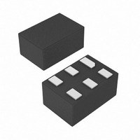
MAX4926ELT+T Maxim Integrated Products, MAX4926ELT+T Datasheet - Page 2

MAX4926ELT+T
Manufacturer Part Number
MAX4926ELT+T
Description
IC CTLR OVP W/EXT PFET 6-UDFN
Manufacturer
Maxim Integrated Products
Datasheet
1.MAX4925ELTT.pdf
(7 pages)
Specifications of MAX4926ELT+T
Applications
*
Mounting Type
Surface Mount
Package / Case
6-µDFN
Lead Free Status / RoHS Status
Lead free / RoHS Compliant
ABSOLUTE MAXIMUM RATINGS
IN, GATE to GND....................................................-0.3V to +30V
FLAG to GND ...........................................................-0.3V to +6V
Continuous Power Dissipation (T
ELECTRICAL CHARACTERISTICS
(V
noted. Typical values are at T
Overvoltage Protectors with
External pFET
Stresses beyond those listed under “Absolute Maximum Ratings” may cause permanent damage to the device. These are stress ratings only, and functional
operation of the device at these or any other conditions beyond those indicated in the operational sections of the specifications is not implied. Exposure to
absolute maximum rating conditions for extended periods may affect device reliability.
Note 1: All devices are 100% tested at +25°C. Electrical limits across the full temperature range are guaranteed by design and characterization.
2
Input Voltage Range
Overvoltage Lockout Level
Overvoltage Lockout Hysteresis
Undervoltage Lockout Level
Undervoltage Lockout Hysteresis
IN Supply Current
GATE Voltage High
GATE Pulldown Current
FLAG Low Voltage
FLAG Leakage Current
TIMING CHARACTERISTICS
Debounce Time
Gate Turn-on Time
Gate Turn-Off Time
Flag Assertion Delay
6-µDFN (derate 2.1mW/°C above 70°C) .......................168mW
IN
_______________________________________________________________________________________
= +5V for MAX4923/MAX4924/MAX4925, V
PARAMETER
A
= +25°C.) (Note 1)
A
= +70°C)
SYMBOL
OVLO
UVLO
t
t
t
I
t
GOFF
V
FLAG
V
GON
V
I
LKG
DEB
I
PD
OH
IN
OL
IN
IN
V
MAX4923
MAX4924
MAX4925
MAX4926
V
MAX4923/MAX4924/MAX4925
MAX4926
V
V
I
V
V
low (Figure 1)
V
(MAX4923/MAX4924/MAX4925) or
V
V
(MAX4923/MAX4924/MAX4925) or from 4V
to 7V (MAX4926) to V
(Figure 1)
V
(MAX4923/MAX4924/MAX4925) or from 4V
to 7V (MAX4926), to V
R
= +4V for MAX4926, C
SINK
IN
IN
IN
GATE
FLAG
UVLO
GATE
GATE
IN
IN
FLAG
rising
falling
> 8V, I
rising at 1V/µs from 5V to 8V
rising at 1V µs from 5V to 8V
= 1mA
= 5.5V
= V
< V
= 5V to 0.5V
= 4V to 0.5V (MAX4926) (Figure 1)
= 10kΩ to 3V (Figure 1)
SOURCE
IN
IN
< V
CONDITIONS
OVLO,
= 0.1mA
Operating Temperature Range ...........................-40°C to +85°C
Junction Temperature .....................................................+150°C
Storage Temperature Range .............................-65°C to +150°C
Lead Temperature (soldering, 10s) ................................+300 °C
GATE
FLAG
MAX4923
MAX4924
MAX4925
MAX4926
time for GATE to go
GATE
= V
= 2.4V,
= 500pF to IN, T
IN
-0.5V
A
2.378
V
MIN
7.00
6.00
5.50
4.35
= -40°C to +85°C, unless otherwise
1.8
0.2
6.5
10
-1
IN
-
2.439
TYP
7.18
6.16
5.65
4.46
0.6
4.5
65
55
50
40
20
14
13
12
20
5
2.500
MAX
28.0
7.36
6.31
5.79
4.57
0.4
+1
25
23
34
20
UNITS
mV
mV
mA
ms
µA
µA
µs
µs
µs
V
V
V
V
V


