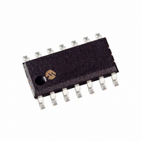
HCS473-I/SL Microchip Technology, HCS473-I/SL Datasheet - Page 54

HCS473-I/SL
Manufacturer Part Number
HCS473-I/SL
Description
IC KEELOQ 3AXIS TRANSCODR 14SOIC
Manufacturer
Microchip Technology
Series
KEELOQ®r
Type
Code Hopping Encoder and Transponderr
Specifications of HCS473-I/SL
Applications
Access Control Systems
Mounting Type
Surface Mount
Package / Case
14-SOIC (3.9mm Width), 14-SOL
Lead Free Status / RoHS Status
Lead free / RoHS Compliant
HCS473
TABLE 7-3:
DS40035C-page 52
AC Characteristics
General HCS473 Timing
T
T
T
T
T
T
Communication from Transponder Reader to HCS473
T
T
T
Response from HCS473 to Transponder Reader
T
T
T
T
T
T
T
T
T
T
Timing Element T
T
Analog delays
T
T
T
T
Note 1: F
Symbol
CMD
SF
AOACK
E
ANTR
ANTF
DB
QUE
PU
PLL
LEDON
LEDOFF
TSCMD
FINH
TSACK
TPACK
WRT
IFF
READ
HOP
DAMP
DEMOD
FILTR
FILTF
2: LF
3: Response timing accounts for T
4: Timing parameters are characterized but not tested.
oscillator variation.
must compensate communication accordingly for T
OSC
1LF
1LF
1LF
TE
1LF
1ms+1LF
is based on the HCS473’s timing, not the timing of the transponder reader. Therefore LF
100 µs
157 µs
205 µs
TE
TE
= 4 MHz may be centered at the designer’s choice of supply voltage (V
67 µs
TE
Min
TE
180
360
720
90
—
—
—
—
—
—
—
—
—
—
—
—
—
AC CHARACTERISTICS, F
+100 µs
+100 µs
+16 µs
-11 µs
E
TE
Hardware design dependent
Hardware design dependent
3.5ms+1LF
1LF
1.2 LF
10.9 ms
16.4 ms
100 ms
500 ms
5.64ms
1 LF
179 µs
227 µs
10 ms
19 ms
1LF
19 ms
89 µs
15 µs
70 µs
TE
4 ms
Typ
100
200
400
800
2s
—
—
+30 µs
TE
TE
TE
FILTR
TE
but not for T
F
The min and max values below are due to HCS473 algorithm tolerances,
not variations due to supply voltage and temperature.
OSC
10ms+1LF
1LF
1LF
OSC
10.2 ms
10.2 ms
212 µs
122 µs
260 µs
10 ms
Preliminary
TE
TE
= 4 MHz
Max
110
220
440
880
—
—
—
—
—
—
—
—
—
—
—
—
—
+44 µs
+11 µs
= 4 MHz
ANTR
ANTR
TE
(1)
or T
and T
Debounce Time
Que Window
Power-up Delay Time (includes button debounce)
Encoder Mode PLL activation to first code word
LED ON Time
LED OFF Time
Delay from Transponder Select ACK to next command
Time to leave LF on after last data bit’s rising edge
Delay to wake-up Acknowledge sequence
Delay from TID pulse rising edge to TID Acknowledge
TID = 0
TID > 0
Delay to Transport Code Acknowledge
Delay to Write Acknowledge
Delay to anticollision off Acknowledge
Delay to IFF response - RF or LF response
Delay to read response - RF or LF response
Delay to hopping code response - RF or LF response
Delay from detecting LC rising edge to first damp pulse
Demodulator mode window looking for edge on LC pin
RFT
RFBSL = LFBSL = 00
RFBSL = LFBSL = 01
RFBSL = LFBSL = 10
RFBSL = LFBSL = 11
HCS473 analog LF filter charge time
HCS473 analog LF filter discharge time
Cumulative LF antenna delay when field is turned on
Cumulative LF antenna delay when field is turned off
ANTF
(1)
ANTF
E
, as they are design dependent. The system designer
or LFT
.
E
DD
) and temperature.
2
2
2
2
Description
2002 Microchip Technology Inc.
TE
is subject to HCS473


