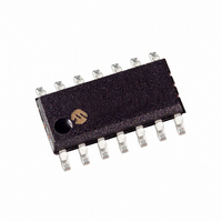
HCS473-I/SL Microchip Technology, HCS473-I/SL Datasheet - Page 17

HCS473-I/SL
Manufacturer Part Number
HCS473-I/SL
Description
IC KEELOQ 3AXIS TRANSCODR 14SOIC
Manufacturer
Microchip Technology
Series
KEELOQ®r
Type
Code Hopping Encoder and Transponderr
Specifications of HCS473-I/SL
Applications
Access Control Systems
Mounting Type
Surface Mount
Package / Case
14-SOIC (3.9mm Width), 14-SOL
Lead Free Status / RoHS Status
Lead free / RoHS Compliant
FIGURE 3-5:
3.1.4.5
The counter select option selects between a 16-bit or
20-bit counter. This option changes the way the 32-bit
hopping portion is constructed, as indicated in
Figure 3-2. The 16-bit counter format additionally
includes two overflow bits for increasing the synchroni-
zation counter range, see Section 3.1.7.
CNTSEL options:
• 16-bit synchronization counter
• 20-bit synchronization counter
3.1.4.6
The HCS473’s battery voltage detector detects when
the supply voltage drops below a predetermined value.
The value is selected by the Low Voltage Trip Point
Select (VLOWSEL) configuration option (Table 3-6).
VLOWSEL options:
• 2.2V trip point
• 3.3V trip point
The low voltage detector result (VLOW) is included in
Hopping code transmissions allowing the receiver to
indicate when the transmitter battery is low (Figure 3-
2). The HCS473 also indicates a low battery condition
by changing the LED operation (Section 3.1.5).
The HCS473 samples the internal low voltage detector
at the end of each code word’s first preamble bit. The
transmitted VLOW status will be a ‘0’ as long as the low
voltage detector indicates V
low voltage trip point. VLOW will change to a ‘1’ if V
drops below the selected low voltage trip point.
TABLE 3-1:
2002 Microchip Technology Inc.
0
1
Code Words
Transmitted
Button Input
VLOW
Sx
Counter Select (CNTSEL)
Low Voltage Trip Point Select
(VLOWSEL)
V
V
DD
DD
VLOW STATUS BIT
is above selected trip voltage
is below selected trip voltage
QUE COUNTER TIMING DIAGRAM
Transmission:
1st Button Press
Description
DD
t ≥ T
is above the selected
DB
QUE1:0 = 00
Synch CNT = X
2
T
Preliminary
DB
DD
All Buttons Released
T
DB
3.1.4.7
The S3/RFEN pin may be configured as an RF enable
output to an RF PLL. The pin’s behavior is coordinated
with the DATA pin to activate a typical PLL in either
ASK or FSK mode.
The PLL Interface (PLLSEL) configuration option con-
trols the output as shown for Encoder operation in
Figure 3-6. Please refer to Section 3.2.8 for RFEN
behavior during LF communication.
PLLSEL options:
• ASK PLL Setup
• FSK PLL Setup
3.1.4.8
The S3/RFEN pin of the HCS473 can be configured to
function as an RF enable output signal. When enabled,
the pin is driven high whenever data is transmitted
through the DATA pin; the S3/RFEN pin can therefore
not be used as an input in this configuration. The RF
enable option bit functions in conjunction with the PLL
interface select option, PLLSEL.
RFEN options:
• S3/RFEN pin functions as S3 switch input only
• S3/RFEN pin functions as RFEN output only
≤ t ≤ T
QUE
PLL Interface Select (PLLSEL)
RF Enable Output (RFEN)
Transmission:
2nd Button Press
HCS473
QUE1:0 = 01
Synch CNT = X+1
DS40035C-page 15
2


