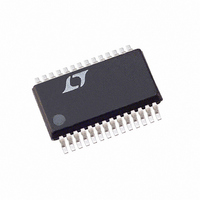
LTC1628IG-PG Linear Technology, LTC1628IG-PG Datasheet - Page 27

LTC1628IG-PG
Manufacturer Part Number
LTC1628IG-PG
Description
IC REG SW 2PHASE STEPDOWN 28SSOP
Manufacturer
Linear Technology
Type
Step-Down (Buck)r
Datasheet
1.LTC1628CGPBF.pdf
(32 pages)
Specifications of LTC1628IG-PG
Internal Switch(s)
No
Synchronous Rectifier
Yes
Number Of Outputs
2
Voltage - Output
Adj to 0.8V
Current - Output
3A
Frequency - Switching
220kHz
Voltage - Input
3.5 ~ 30 V
Operating Temperature
-40°C ~ 85°C
Mounting Type
Surface Mount
Package / Case
28-SSOP
Lead Free Status / RoHS Status
Contains lead / RoHS non-compliant
Power - Output
-
Available stocks
Company
Part Number
Manufacturer
Quantity
Price
Part Number:
LTC1628IG-PG#PBF
Manufacturer:
LINEAR/凌特
Quantity:
20 000
APPLICATIO S I FOR ATIO
PC Board Layout Checklist
When laying out the printed circuit board, the following
checklist should be used to ensure proper operation of the
LTC1628. These items are also illustrated graphically in
the layout diagram of Figure 10. The Figure 11 illustrates
the current waveforms present in the various branches of
the 2-phase synchronous regulators operating in the
continuous mode. Check the following in your layout:
1. Are the top N-channel MOSFETs M1 and M3 located
within 1cm of each other with a common drain connection
at C
two channels as it can cause a large resonant loop.
IN
? Do not attempt to split the input decoupling for the
*PGOOD ON THE LTC1628-PG
R1
R3
U
INTV
R2
R4
CC
U
3.3V
Figure 10. LTC1628 Recommended Printed Circuit Layout Diagram
10
11
12
13
14
1
2
3
4
5
6
7
8
9
W
RUN/SS1
SENSE1
SENSE1
V
FREQSET
STBYMD
FCB
I
SGND
3.3V
I
V
SENSE2
SENSE2
TH1
TH2
OSENSE1
OSENSE2
OUT
LTC1628
+
–
–
+
(PGOOD)*
RUN/SS2
BOOST1
BOOST2
FLTCPL
EXTV
INTV
U
PGND
SW1
SW2
TG1
BG1
BG2
TG2
V
CC
CC
IN
FLTCPL
28
27
26
25
24
23
22
21
20
19
18
17
16
15
2. Are the signal and power grounds kept separate? The
combined LTC1628 signal ground pin and the ground
return of C
terminals. The path formed by the top N-channel MOSFET,
Schottky diode and the C
leads and PC trace lengths. The output capacitor (–)
terminals should be connected as close as possible to the
(–) terminals of the input capacitor by placing the capaci-
tors next to each other and away from the Schottky loop
described above.
3. Do the LTC1628 V
nect to the (+) terminals of C
must be connected between the (+) terminal of C
R
PGOOD
PU
C
C
C
B1
B2
INTVCC
V
(<7V)
PULL-UP
INTVCC
LTC1628/LTC1628-PG
C
VIN
V
R
IN
M1
IN
M3
must return to the combined C
OSENSE
M2
M4
L1
C
L2
IN
IN
capacitor should have short
pins resistive dividers con-
R
R
OUT
SENSE
SENSE
C
C
OUT1
OUT2
D1
D2
? The resistive divider
1628 F10
V
GND
V
OUT1
OUT2
OUT
27
OUT
1628fb
and
(–)


