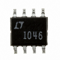
LTC1046CS8 Linear Technology, LTC1046CS8 Datasheet - Page 7

LTC1046CS8
Manufacturer Part Number
LTC1046CS8
Description
IC CMOS VOLT CONV SW-CAP 8-SOIC
Manufacturer
Linear Technology
Type
Switched Capacitor (Charge Pump), Divider, Invertingr
Datasheet
1.LTC1046CN8PBF.pdf
(12 pages)
Specifications of LTC1046CS8
Internal Switch(s)
Yes
Synchronous Rectifier
No
Number Of Outputs
1
Current - Output
50mA
Frequency - Switching
5.5kHz ~ 30kHz
Voltage - Input
1.5 ~ 6 V
Operating Temperature
0°C ~ 70°C
Mounting Type
Surface Mount
Package / Case
8-SOIC (3.9mm Width)
Output Voltage
-1.5 to -6/0.75 to 3V
Output Current
50mA
Operating Supply Voltage (min)
1.5V
Operating Supply Voltage (max)
6V
Operating Temp Range
0C to 70C
Operating Temperature Classification
Commercial
Package Type
SOIC N
Pin Count
8
Mounting
Surface Mount
Lead Free Status / RoHS Status
Contains lead / RoHS non-compliant
Voltage - Output
-
Power - Output
-
Lead Free Status / Rohs Status
Not Compliant
Available stocks
Company
Part Number
Manufacturer
Quantity
Price
Company:
Part Number:
LTC1046CS8
Manufacturer:
LINEAR
Quantity:
16 000
Part Number:
LTC1046CS8
Manufacturer:
LINEAR/凌特
Quantity:
20 000
Company:
Part Number:
LTC1046CS8#PBF
Manufacturer:
LTC
Quantity:
810
Part Number:
LTC1046CS8#PBF
Manufacturer:
LINEAR/凌特
Quantity:
20 000
Company:
Part Number:
LTC1046CS8#TR
Manufacturer:
LT
Quantity:
623
Part Number:
LTC1046CS8#TRPBF
Manufacturer:
LT/凌特
Quantity:
20 000
Negative Voltage Converter
Figure 7 shows a typical connection which will provide a
negative supply from an available positive supply. This
circuit operates over full temperature and power supply
ranges without the need of any external diodes. The LV pin
(Pin 6) is shown grounded, but for V
floated, since LV is internally switched to GND (Pin 3) for
V
The output voltage (Pin 5) characteristics of the circuit are
those of a nearly ideal voltage source in series with an 27
resistor. The 27 output impedance is composed of two
terms: 1) the equivalent switched capacitor resistance
(see Theory of Operation), and 2) a term related to the ON
resistance of the MOS switches.
At an oscillator frequency of 30kHz and C1 = 10 F, the first
term is:
Notice that the equation for R
reactance equation (X
term.
The exact expression for output impedance is complex,
but the dominant effect of the capacitor is clearly shown on
TYPICAL
+
R
15 10
3V.
EQUIV
10 F
•
+
=
3
Figure 7. Negative Voltage Converter
•
A
1
10 10
f
OSC
PPLICATI
1
2
3
4
•
BOOST
CAP
GND
CAP
/ 2
T
1
MIN
LTC1046
C
+
–
–
= 1/ C) and does not contain a 2
6
•
T
C1
V
A
OSC
OUT
V
LV
+
T
6 7
MAX
.
8
7
6
5
O
EQUIV
REQUIRED FOR V
U
+
S
1046 F07
is not a capacitive
10 F
+
V
1.5V TO 6V
V
OUT
+
3V, it may be
+
= –V
< 3V
+
the typical curves of output impedance and power effi-
ciency versus frequency. For C1 = C2 = 10 F, the output
impedance goes from 27 at f
f
switch ON resistance term, the output resistance is deter-
mined by 1/fC only.
Voltage Doubling
Figure 8 shows a two diode, capacitive voltage doubler.
With a 5V input, the output is 9.1V with no load and 8.2V
with a 10mA load.
Ultraprecision Voltage Divider
An ultraprecision voltage divider is shown in Figure 9. To
achieve the 0.0002% accuracy indicated, the load current
should be kept below 100nA. However, with a slight loss
in accuracy, the load current can be increased.
OSC
= 1kHz. As the 1/fC term becomes large compared to
V
T
I
2
L
MIN
+
1
2
3
4
100nA
0.002%
BOOST
CAP
GND
CAP
T
Figure 9. Ultraprecision Voltage Divider
A
10 F
LTC1046
C1
+
–
T
MAX
+
V
OSC
Figure 8. Voltage Doubler
OUT
V
LV
+
+
8
7
6
5
1
2
3
4
C2
10 F
BOOST
CAP
GND
CAP
LTC1046
REQUIRED
FOR
V
+
–
+
< 3V
V
OSC
OUT
V
LV
REQUIRED FOR V
OSC
+
V
D
+
+
8
7
6
5
= 30kHz to 225 at
+
10 F
V
V
3V TO 12V
1046 F09
D
+
+
+
LTC1046
< 6V
1046 F08
10 F
V
1.5V TO 6V
V
(V
OUT
+
IN
– 1)
= 2
1046fb
7


