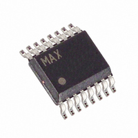
MAX1831EEE Maxim Integrated Products, MAX1831EEE Datasheet - Page 11

MAX1831EEE
Manufacturer Part Number
MAX1831EEE
Description
IC REG STEP-DWN 3A W/SW 16-QSOP
Manufacturer
Maxim Integrated Products
Type
Step-Down (Buck)r
Datasheet
1.MAX1831EEE.pdf
(13 pages)
Specifications of MAX1831EEE
Internal Switch(s)
Yes
Synchronous Rectifier
Yes
Number Of Outputs
1
Voltage - Output
1.5V, 2.5V, 3.3V, Adj
Current - Output
3A
Frequency - Switching
1MHz
Voltage - Input
3 ~ 5.5 V
Operating Temperature
-40°C ~ 85°C
Mounting Type
Surface Mount
Package / Case
16-QSOP
Power - Output
1.12W
Output Voltage
1.5 V to 3.3 V
Output Current
3.4 A
Input Voltage
3 V to 5.5 V
Switching Frequency
1 MHz
Maximum Operating Temperature
+ 85 C
Minimum Operating Temperature
- 40 C
Lead Free Status / RoHS Status
Contains lead / RoHS non-compliant
Available stocks
Company
Part Number
Manufacturer
Quantity
Price
Company:
Part Number:
MAX1831EEE
Manufacturer:
MAXIM
Quantity:
60
Part Number:
MAX1831EEE
Manufacturer:
MAXIM/美信
Quantity:
20 000
Figure 5. Maximum Recommended Continuous Output Current
vs. Temperature
An internal transconductance amplifier fine tunes the
output DC accuracy. A capacitor, C
to V
For stability, choose C
A large capacitor value maintains a constant average
output voltage but slows the loop response to changes
in output voltage. A small capacitor value speeds up
the loop response to changes in output voltage but
decreases stability.
High ambient temperatures can limit the maximum
current or duty factor of the output current, depending
on the total copper, are connected to the MAX1830/
MAX1831 and available airflow.
Figure 5 shows the maximum recommended continuous
output current vs. ambient temperature. Figure 6 shows
the maximum recommended output current vs. the out-
put current duty cycle at high temperatures. These fig-
ures are based on 0.7in
Figure 6 assumes that the output current is a square
wave with a 100Hz frequency. The duty cycle is
defined as the duration of the burst current divided by
the period of the square wave. This figure shows the
limitations for continuous bursts of output current.
Note that if the thermal limitations of the MAX1830/
MAX1831 are exceeded, it enters thermal shutdown to
prevent destructive failure.
3A, 1MHz, Low-Voltage, Step-Down Regulators with
CC
Synchronous Rectification and Internal Switches
High-Current Thermal Considerations
compensates the transconductance amplifier.
3.50
3.40
3.30
3.20
3.10
3.00
2.90
2.80
2.70
2.60
2.50
2.40
MAXIMUM RECOMMENDED CONTINUOUS
25
OUTPUT CURRENT vs. TEMPERATURE
0.7IN
35
2
______________________________________________________________________________________
OF 1-OZ COPPER
MAX1830/MAX1831
TEMPERATURE (°C)
COMP
45
2
of 1oz copper in free air.
55
= 470pF.
Integrator Amplifier
65
COMP
75
, from COMP
85
The operating frequency of the MAX1830/MAX1831 is
determined primarily by t
V
However, as the output current increases, the voltage
drop across the NMOS and PMOS switches increases
and the voltage across the inductor decreases. This
causes the frequency to drop. The change in frequency
can be approximated with the following formula:
where R
(50mΩ typ).
Good layout is necessary to achieve the MAX1830/
MAX1831s’ intended output power level, high efficien-
cy, and low noise. Good layout includes the use of a
ground plane, careful component placement, and cor-
rect routing of traces using appropriate trace widths.
Figure 6. Maximum Recommended Burst Current vs. Burst
Current Duty Cycle
OUT
as shown in the following formula:
PMOS
f
PWM
3.40
3.20
3.00
2.80
2.60
2.40
∆f
MAXIMUM RECOMMENDED BURST CURRENT
PWM
0
=
is the resistance of the internal MOSFETs
I
FROM 1A TO THE BURST CURRENT
OUT
vs. BURST CURRENT DUTY CYCLE
[
t
= -I
OFF
IS A 100Hz SQUARE WAVE
Circuit Layout and Grounding
20
(
V
OUT
(
IN
V
IN
−
Frequency Variation with
DUTY CYCLE (%)
T
A
−
V
x R
40
= +85°C
OUT
V
OFF
PMOS
PMOS
−
(set by R
60
V
+
PMOS
V
/ (V
NMOS
T
A
Output Current
80
= +55°C
IN
)
x t
TOFF
)
]
OFF
100
), V
)
IN
, and
11


