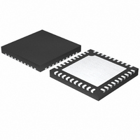
MAX1566ETL+ Maxim Integrated Products, MAX1566ETL+ Datasheet - Page 33

MAX1566ETL+
Manufacturer Part Number
MAX1566ETL+
Description
IC DGTL CAM PWR-SUP 6CH 40TQFN
Manufacturer
Maxim Integrated Products
Datasheet
1.MAX1567ETLT.pdf
(35 pages)
Specifications of MAX1566ETL+
Applications
Controller, Digital Camera
Voltage - Input
0.7 ~ 5.5 V
Number Of Outputs
7
Voltage - Output
1.25 ~ 5 V
Operating Temperature
-40°C ~ 85°C
Mounting Type
Surface Mount
Package / Case
40-TQFN Exposed Pad
Lead Free Status / RoHS Status
Lead free / RoHS Compliant
If different magnitudes are required for the positive and
negative voltages, a linear regulator can be used at
one of the outputs to achieve the desired voltages. One
such connection is shown in Figure 12. This circuit is
somewhat unique in that a positive-output linear regu-
lator can regulate a negative voltage output. It does this
by controlling the charge current flowing to the flying
capacitor rather than directly regulating at the output.
The MAX1566/MAX1567s’ internal switch step-up,
main, and step-down converters can be cascaded to
make a high-efficiency boost-buck converter, but it is
sometimes desirable to build a second boost-buck
converter with an AUX_ controller.
One type of step-up/step-down converter is the SEPIC,
shown in Figure 13. Inductors L1 and L2 can be sepa-
rate inductors or can be wound on a single core and
coupled like a transformer. Typically, a coupled inductor
improves efficiency since some power is transferred
through the coupling so less power passes through the
coupling capacitor (C2). Likewise, C2 should have low
ESR to improve efficiency. The ripple-current rating must
be greater than the larger of the input and output cur-
rents. The MOSFET (Q1) drain-source voltage rating and
the rectifier (D1) reverse-voltage rating must exceed the
sum of the input and output voltages. Other types of
step-up/step-down circuits are a flyback converter and a
step-up converter followed by a linear regulator.
The MAX1801 is a 6-pin, SOT-slave, DC-to-DC controller
that can be connected to generate additional output volt-
ages. It does not generate its own reference or oscillator.
Instead, it uses the reference and oscillator of the
MAX1566/MAX1567 (Figure 14). The MAX1801 controller
operation and design are similar to that of the
MAX1566/MAX1567 AUX controllers. All comments in the
AUX Controller Component Selection section also apply
to add-on MAX1801 slave controllers. For more details,
refer to the MAX1801 data sheet.
The MAX1566/MAX1567 have three status outputs:
SDOK, AUX1OK, and SCF. These monitor the output of
the step-down channel, the AUX1 channel, and the sta-
tus of the overload-short-circuit protection. Each output
is open drain to allow the greatest flexibility. Figures 15,
16, and 17 show some possible connections for these
outputs.
Applications for Status Outputs
______________________________________________________________________________________
Adding a MAX1801 Slave
Six-Channel, High-Efficiency, Digital
SEPIC Boost-Buck
Camera Power Supplies
SDOK goes low when the step-down reaches regula-
tion. Some microcontrollers with low-voltage cores
require that the high-voltage (3.3V) I/O rail not be pow-
ered up until the core has a valid supply. The circuit in
Figure 15 accomplishes this by driving the gate of a
PFET connected between the 3.3V output and the
processor I/O supply.
Figure 16 shows a similar application where AUX1OK
gates 5V power to the CCD only after the +15V output
is in regulation.
Alternately, power sequencing can also be implement-
ed by connecting RC networks to delay the appropriate
converter ON_ inputs.
The SCF output goes low only after the step-up reaches
regulation. It can be used to drive a P-channel MOSFET
switch that turns off the load of a selected supply in the
event of an overload. Or, it can remove the load until
the supply reaches regulation, effectively allowing full-
load startup. Figure 17 shows such a connection for the
step-up output.
The step-down feedback voltage is 1.25V. With a stan-
dard two-resistor feedback network, the output voltage
can be set to values between 1.25V and the input volt-
age. If a step-down output voltage less than 1.25V is
desired, it can be set by adding a third feedback resis-
tor from FBSD to a voltage higher than 1.25V. The step-
up or main outputs are convenient for this, as shown in
Figure 18.
The equation governing output voltage in Figure 18’s
circuit is as follows:
where V
V
age that is higher than 1.25V can be used as the con-
nection point for R3 in Figure 18, and for the V
in the equation. Since there are multiple solutions for
R1, R2, and R3, the above equation cannot be written
in terms of one resistor. The best method for determin-
ing resistor values is to enter the above equation into a
spreadsheet and test estimated resistor values. A good
starting point is with 100kΩ at R2 and R3.
SU
Using
0 = [(V
is the step-up output voltage. Any available volt-
SD
[(V
SDOK and AUX1OK for Power Sequencing
SD
SU
is the output voltage, V
- V
- V
FBSD
FBSD
Using SCF for Full-Load Startup
) / R1] + [(0 - V
) / R3]
Setting V
SD
FBSD
FBSD
Below 1.25V
is 1.25V, and
) / R2] +
SD
term
33


