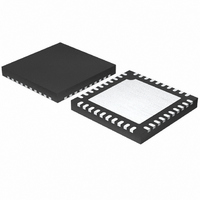
MAX1566ETL+ Maxim Integrated Products, MAX1566ETL+ Datasheet - Page 30

MAX1566ETL+
Manufacturer Part Number
MAX1566ETL+
Description
IC DGTL CAM PWR-SUP 6CH 40TQFN
Manufacturer
Maxim Integrated Products
Datasheet
1.MAX1567ETLT.pdf
(35 pages)
Specifications of MAX1566ETL+
Applications
Controller, Digital Camera
Voltage - Input
0.7 ~ 5.5 V
Number Of Outputs
7
Voltage - Output
1.25 ~ 5 V
Operating Temperature
-40°C ~ 85°C
Mounting Type
Surface Mount
Package / Case
40-TQFN Exposed Pad
Lead Free Status / RoHS Status
Lead free / RoHS Compliant
Six-Channel, High-Efficiency, Digital
Camera Power Supplies
For the example:
Since ceramic capacitors are common in either 22µF or
47µF values, 22µF is within a factor of two of the ideal value
and still provides adequate phase margin for stability. If
the output filter capacitor has significant ESR, a zero
occurs at the following:
If Z
with ceramic output capacitors. If Z
be cancelled with a pole set by capacitor C
ed from C
If C
All MAX1566/MAX1567 AUX controllers drive external
logic-level MOSFETs. Significant MOSFET selection
parameters are as follows:
• On-resistance (R
• Maximum drain-to-source voltage (V
• Total gate charge (Q
• Reverse transfer capacitance (C
On the MAX1566, all AUX drivers are designed for N-
channel MOSFETs. On the MAX1567, AUX2 is a DC-to-
DC inverter, so DL2 is designed to drive a P-channel
MOSFET. In both devices, the driver outputs DL1 and
DL3 swing between PVSU and GND. MOSFET driver
DL2 swings between INDL2 and GND.
Use a MOSFET with on-resistance specified with gate
drive at or below the main output voltage. The gate
charge, Q
charging the gate and helps to predict MOSFET transi-
tion time between on and off states. MOSFET power
dissipation is a combination of on-resistance and tran-
sition losses. The on-resistance loss is as follows:
where D is the duty cycle, I
current, and R
transition loss is approximately as follows:
where V
inductor current, f
t
mately Q
I
30
T
G
is the transition time. The transition time is approxi-
is the gate-drive current (0.5A typ).
ESR
P
______________________________________________________________________________________
is calculated to be <10pF, it can be omitted.
AUX Controller Component Selection
> f
C
OUT
G
OUT
C
P
G
C
/ I
TRANS
to GND:
, includes all capacitance associated with
, it can be ignored, as is typically the case
Z
G
P
is the output voltage, I
ESR
= 27kΩ x 6.8nF / 5.14Ω = 35.7µF
, where Q
RDSON
DS(ON)
C
P
= 1 / (2π x C
= (V
OSC
= C
DS(ON)
= D x I
OUT
OUT
is the switching frequency, and
is MOSFET on-resistance. The
G
G
)
)
is the total gate charge, and
x I
x R
L
L
L
2
OUT
ESR
x f
is the average inductor
x R
OSC
DS(ON)
x R
/ R
RSS
ESR
External MOSFET
C
L
x t
ESR
)
DS(MAX)
is the average
T
< f
) / 3
)
C
P
, it should
connect-
)
The total power dissipation in the MOSFET is as follows:
For most AUX applications, a Schottky diode rectifies
the output voltage. Schottky low forward voltage and
fast recovery time provide the best performance in
most applications. Silicon signal diodes (such as
1N4148) are sometimes adequate in low-current
(<10mA), high-voltage (>10V) output circuits where the
output voltage is large compared to the diode forward
voltage.
The auxiliary controllers employ voltage-mode control
to regulate their output voltage. Optimum compensa-
tion depends on whether the design uses continuous or
discontinuous inductor current.
When the inductor current falls to zero on each switch-
ing cycle, it is described as discontinuous. The inductor
is not utilized as efficiently as with continuous current,
but in light-load applications this often has little negative
impact since the coil losses may already be low com-
pared to other losses. A benefit of discontinuous induc-
tor current is more flexible loop compensation, and no
maximum duty-cycle restriction on boost ratio.
To ensure discontinuous operation, the inductor must
have a sufficiently low inductance to fully discharge on
each cycle. This occurs when:
A discontinuous current boost has a single pole at the
following:
Choose the integrator cap so the unity-gain crossover,
f
circuits, such as those powering motors, LEDs, or other
loads that do not require fast transient response, it is
often acceptable to overcompensate by setting f
f
C
where:
and V
ramp of 1.25V.
C
OSC
C
C
, occurs at f
C
L < [V
f
is then determined by the following:
P
= [2V
/ 20 or lower.
= (2V
RAMP
AUX Step-Up, Discontinuous Inductor Current
(K(V
IN
OUT
2
OUT
OUT
is the internal slope-compensation voltage
P
(V
OSC
MOSFET
x V
OUT
- V
- V
K = 2L x f
IN
/ 10 or lower. Note that for many AUX
IN
IN
- V
/ ((2V
) / (2π x R
))]
= P
IN
1/2
) / V
RDSON
OUT
[(V
OSC
OUT
FB
LOAD
- V
/ R
/ V
3
+ P
IN
] [R
LOAD
OUT
AUX Compensation
) x V
x C
TRANS
LOAD
)(g
OUT
RAMP
M
/ (2f
/ (2π x f
x V
)] [V
OSC
OUT
OUT
Diode
)]
C
)
C
))]
at
/


