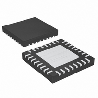
MAX1904ETJ+T Maxim Integrated Products, MAX1904ETJ+T Datasheet - Page 18

MAX1904ETJ+T
Manufacturer Part Number
MAX1904ETJ+T
Description
IC CNTRLR PWR SPLY LN 32-TQFN
Manufacturer
Maxim Integrated Products
Datasheet
1.MAX1904ETJ.pdf
(33 pages)
Specifications of MAX1904ETJ+T
Applications
Controller, Notebook Computers
Voltage - Input
4.2 ~ 30 V
Number Of Outputs
4
Voltage - Output
2.5 ~ 5 V
Operating Temperature
0°C ~ 85°C
Mounting Type
Surface Mount
Package / Case
32-TQFN Exposed Pad
Output Voltage
3.3 V, 5 V, 2.5 V to 5.5 V
Output Current
5 A
Input Voltage
4.2 V to 30 V
Mounting Style
SMD/SMT
Maximum Operating Temperature
+ 85 C
Minimum Operating Temperature
- 40 C
Lead Free Status / RoHS Status
Lead free / RoHS Compliant
The power-good monitor generates a system RESET
signal. At first power-up, RESET is held low until both
the 3.3V and 5V SMPS outputs are in regulation. At this
point, an internal timer begins counting oscillator puls-
es, and RESET continues to be held low until 32,000
cycles have elapsed. After this timeout period (64ms at
500kHz or 96ms at 333kHz), RESET is actively pulled
up to V
controls), only the 3.3V SMPS is monitored—the 5V
SMPS is ignored.
The output undervoltage lockout circuit is similar to
foldback current limiting, but employs a timer rather
than a variable current limit. Each SMPS has an under-
voltage protection circuit that is activated 6144 clock
cycles after the SMPS is enabled. If either SMPS output
is under 70% of the nominal value, both SMPSs are
latched off and their outputs are clamped to ground by
the synchronous rectifier MOSFETs (see the Output
Overvoltage Protection section). They won’t restart until
SHDN or RUN/ON3 is toggled, or until V+ power is
cycled below 1V. Note that undervoltage protection can
make prototype troubleshooting difficult, since you
have only 12ms or 18ms to figure out what might be
wrong with the circuit before both SMPSs are latched
off. In extreme cases, it may be useful to substitute the
MAX1904 into the prototype breadboard until the proto-
type is working properly.
500kHz Multi-Output, Low-Noise Power-Supply
Controllers for Notebook Computers
Table 4. Operating Modes
18
SHDN
High
High
High
High
High
High
High
High
Low
______________________________________________________________________________________
L
. If SEQ is tied to REF (for separate ON3/ON5
RESET Power-Good Voltage Monitor
SEQ
GND
GND
REF
REF
REF
REF
VL
VL
Protection (MAX1901/MAX1902)
X
Output Undervoltage Shutdown
RUN/ON3
High
High
High
High
Low
Low
Low
Low
X
Timing Capacitor
Timing Capacitor
Timing Capacitor
Timing Capacitor
TIME/ON5
High
High
Low
Low
X
Shutdown
Standby
Standby
Standby
MODE
Both SMPS outputs are monitored for overvoltage. If
either output is more than 7% above the nominal regu-
lation point, both low-side gate drivers (DL_) are
latched high until SHDN or RUN/ON3 is toggled, or
until V+ power is cycled below 1V. This action turns on
the synchronous rectifiers with 100% duty, in turn rapid-
ly discharging the output capacitors and forcing both
SMPS outputs to ground. The DL outputs are also kept
high whenever the corresponding SMPS is disabled,
and in shutdown if V
Discharging the output capacitor through the main
inductor causes the output to momentarily go below
GND. Clamp this negative pulse with a back-biased 1A
Schottky diode across the output capacitor (Figure 1).
To ensure overvoltage protection on initial power-up,
connect signal diodes from both output voltages to V
(cathodes to V
This circuitry protects the load from accidental overvolt-
age caused by a short circuit across the high-side
power MOSFETs. This scheme relies on the presence
of a fuse, in series with the battery, which is blown by
the resulting crowbar current. Note that the overvoltage
circuitry will interfere with external keep-alive supplies
that hold up the outputs (such as lithium backup or hot-
swap power supplies); in such cases, the MAX1904
should be used.
PWM mode (SKIP = high) minimizes RF and audio inter-
ference in noise-sensitive applications (such as hi-fi multi-
media-equipped systems), cellular phones, RF
communicating computers, and electromagnetic pen
entry systems. See the summary of operating modes in
Table 2. SKIP can be driven from an external logic signal.
Run
Run
Run
Run
Run
All circuit blocks turned off.
Supply current = 4µA.
Both SMPSs off. Supply current = 30µA.
Both SMPSs enabled. 3.3V enabled Before 5V.
Both SMPSs off. Supply current = 30µA.
3.3V SMPS enabled/5V off.
5V SMPS enabled/3.3V off.
Both SMPSs enabled.
Both SMPSs off. Supply current = 30µA.
Both SMPSs enabled. 5V enabled before 3.3V.
Low-Noise Operation (PWM Mode)
L
Output Overvoltage Protection
) to eliminate the V
L
is sustained.
DESCRIPTION
(MAX1901/MAX1902)
L
power-up delay.
L


